TL072 Op Amp pinout, Circuit, Equivalent and Package
Author:admin Date: 2025-04-18 06:32 Views:109
Operational amplifier output voltage swing test – NE5532, TL072, LM4562 and more
In the world of analog electronics, operational amplifiers (op-amps) are essential building blocks. Among them, the TL072 op amp stands out as a dual low-noise JFET-input operational amplifier designed for high-performance audio and signal processing tasks. Thanks to its low input bias current, high slew rate, and broad bandwidth, the TL072 excels in applications where precision, speed, and signal clarity are critical.
This comprehensive guide covers everything you need to know about the TL072 op amp, including its internal working, pin configuration, popular circuit examples, practical applications, and compatible alternatives.
What is the TL072 Op Amp?
The TL072 is a dual operational amplifier IC belonging to the popular TL07x series, which also includes:
TL071 – single op amp
TL072 – dual op amp
TL074 – quad op amp
All members of the TL07x family feature JFET-input stages, offering high input impedance and low input bias current. These characteristics make the TL072 especially suitable for interfacing with high-impedance sources, such as guitar pickups, audio sensors, and measurement systems.
Key Technical Overview:
Before diving into the circuitry, it’s important to understand the TL072’s technical specifications:
Architecture: Dual op-amp with JFET inputs
Supply Voltage Range: ±3V to ±18V
Slew Rate: 13 V/µs (typical)
Unity-Gain Bandwidth: 3 MHz
Input Offset Voltage: ~3 mV
Total Harmonic Distortion (THD): 0.003% typical
Low Power Consumption: Internally compensated for stability
Package Options: DIP, SOIC, TSSOP
TL072 Key Features:
The TL072 offers a combination of features that make it a go-to choice for both audio and general-purpose analog designs:
Low Noise: Ideal for audio and precision signal processing
High Slew Rate: Ensures fast and accurate signal response
Wide Bandwidth: Great for high-frequency applications
JFET Inputs: High impedance, minimal signal loading
Low Input Bias Current: ~65 pA typical
Wide Voltage Range: Versatile for dual- and single-supply systems
Internally Compensated: No need for external compensation
Drop-in Compatible: Commonly used in legacy and modern designs alike
TL072 Working Principle
At its core, the TL072 functions as a dual voltage amplifier, amplifying the voltage difference between its input terminals. It consists of:
1. A JFET-input differential stage, offering high input impedance
2. A high-gain amplifier stage for signal boosting
3. A Class AB push-pull output driver for low impedance drive
This internal structure ensures low noise, fast response, and excellent linearity, which are critical in precision analog circuits.
How Does the TL072 Work?
The TL072 is a dual operational amplifier (op amp) designed with JFET-input stages. This structure offers high input impedance, low input bias current, and excellent frequency response—making it ideal for analog signal processing.
Internally, each amplifier within the TL072 consists of three main stages:
Input Stage (Differential Amplifier)
This stage uses junction field-effect transistors (JFETs) as input devices. It senses the voltage difference between the inverting (−) and non-inverting (+) inputs. Because of the JFETs, the input draws very little current—resulting in high input impedance and minimal loading of the signal source.
Gain Stage (Voltage Amplification)
The difference detected at the input is amplified by a high-gain voltage amplifier. This middle stage ensures that even small input signals can result in a significant output swing. Compensation circuitry is used here to control frequency stability.
Output Stage (Class AB Output Driver)
The output stage is typically a push-pull configuration, enabling the TL072 to drive low-impedance loads efficiently. It ensures a low output impedance and provides the necessary current to the output load while maintaining linearity.
In operation, the TL072 amplifies the difference between the two inputs, rejecting any voltage that is common to both (common-mode). This makes it well-suited for filtering, buffering, and amplification tasks where signal integrity is critical.
Thanks to its low noise, high slew rate, and low total harmonic distortion (THD), the TL072 is widely used in audio preamps, active filters, and instrumentation circuits.
TL072 Pinout and Internal Schematic
The TL072 is packaged in a standard 8-pin configuration. Here’s the pinout:

| Pin Number | Function | Description |
|---|---|---|
| 1 | Output A | Output of Op-Amp A |
| 2 | Inverting Input A (-) | Inverting input of Op-Amp A |
| 3 | Non-Inverting Input A (+) | Non-inverting input of Op-Amp A |
| 4 | V- (GND) | Negative power supply (ground) |
| 5 | Non-Inverting Input B (+) | Non-inverting input of Op-Amp B |
| 6 | Inverting Input B (-) | Inverting input of Op-Amp B |
| 7 | Output B | Output of Op-Amp B |
| 8 | V+ | Positive power supply |
Internally, the TL072 uses matched JFET pairs and active load circuits to deliver balanced performance across both channels.
TL072 Circuit Design Example
The TL072 excels in various classic op-amp configurations. Here are four of the most commonly used:
1. Non-Inverting Amplifier

The input signal is applied to the non-inverting input (+) of the TL072. The inverting input (−) is connected to a voltage divider made up of feedback resistor Rf and ground resistor Rg. The output feeds back to the divider.
Working Principle:
1. The op-amp operates to maintain the voltage at both inputs equal.
2. Since the inverting input is connected to a divided version of the output, the op-amp adjusts Vout so that:
Vin=V–= Rg /(Rf+Rg)·Vout
3. Solving this gives the closed-loop voltage gain:
Au= Vin/Vout=1+Rf/Rg
Design Notes:
1. Typical Resistors:
Rf=47kΩ,Rg=4.7kΩR → Gain ≈ 11.
2. Input Impedance: Very high (>1 MΩ), ideal for signal sources that can’t supply much current.
3. Bandwidth Consideration: Higher gain reduces bandwidth due to gain-bandwidth product (GBWP ≈ 3 MHz for TL072).
4. Stability Tip: For gains above 10, consider a compensation capacitor (~10pF) across Rf
2. Inverting Amplifier
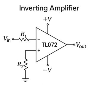
The signal is applied via resistor Rin to the inverting input (−). The non-inverting input (+) is grounded. A feedback resistor Rf connects the output back to the inverting input.
Working Principle:
1. The op-amp maintains a “virtual ground” at the inverting input. The voltage at (−) is nearly 0V.
2. The current through Rin is:
Iin=Vin/Rin
3. This current flows through Rf, producing:
Vout=−Iin·Rf=−Rf/Rin·Vin
4. Thus, the gain is:
Au=−Rf/Rin
Design Notes:
1. Typical Resistors:
Rin=10kΩ,Rf=100kΩ → Gain = −10.
2. Phase Behavior: Signal is 180° out of phase with input.
3. Input Impedance: Equal to Rin. Choose carefully if driving from a high-impedance source.
4. Noise Tip: Keep resistor values below 100kΩ to reduce thermal noise.
3. Voltage Follower

The input is connected directly to the non-inverting input (+). The output is looped back to the inverting input (−). No resistors are needed.
Working Principle:
1. The op-amp forces the output voltage to track the input voltage exactly.
2. Since both inputs are effectively equal, the voltage difference is zero, and output equals input:
Vout= Vin
3. This configuration has unity gain and no phase inversion.
Design Notes:
1. Input Impedance: Extremely high (>10⁹ Ω), minimal loading on signal sources.
2. Output Impedance: Very low (~100Ω or less), can drive moderate loads directly.
3. Bandwidth: Very wide since gain is 1; TL072’s full open-loop bandwidth is nearly preserved.
4. Slew Rate: TL072 provides a typical slew rate of 13V/µs, making it suitable for fast signal transitions.
4. Summing Amplifier
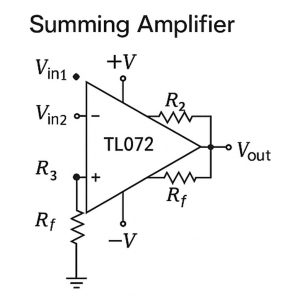
Multiple input voltages (V1,V2,…) are connected through resistors R1,R2,… to the inverting input (−). The non-inverting input (+) is grounded. A single feedback resistor Rf connects the output to the inverting input.
Working Principle:
1. Each input produces a current In=Vn/Rn, all of which sum at the inverting node.
2. Since the inverting input is a virtual ground, these currents combine and flow through Rf, resulting in:
Vout=-Rf(V1/R1+V2/R2+⋯)
3. If all Rn are equal, the result is a scaled inverted sum.
Design Notes:
1. Typical Resistors:
R1=R2=R3=10kΩ,Rf=10kΩ
2. Gain Control: Adjust individual input resistors to control weight of each input.
3. Power Supply Decoupling: Place 100nF caps close to Vcc and Vee pins for stability.
4. Parasitics Tip: Keep summing node traces short to avoid noise pickup or oscillation.
TL072 Voltage Requirements
The TL072 operates with:
1. Dual supply: Typically ±15V (range: ±3V to ±18V)
2. Single supply: 5V to 36V (with reduced swing near GND)
Always add 0.1μF and 10μF capacitors close to the supply pins to ensure power stability.
Applications of TL072
Let’s explore where the TL072 op amp excels in real-world circuits:
Audio Preamplifiers
TL072 is a top choice for audio preamp circuits, mixers, and headphone amplifiers. Its low distortion and wide bandwidth deliver clean audio signals in both professional and DIY audio projects.
Active Filters
Ideal for designing active filters (low-pass, high-pass, band-pass), the TL072 ensures stable performance in audio equalizers, tone control circuits, and signal conditioning systems.
Oscillator Circuits
Used in oscillator designs for waveform generation, TL072 can produce clean sine, triangle, and square waves in function generators and test equipment.
Buffer Amplifiers
With high input impedance and unity-gain stability, TL072 is excellent as a voltage follower or buffer amplifier in ADC interfaces, sensor outputs, and analog isolation circuits.
Analog Signal Processing
TL072 is commonly used in analog signal processing applications, including integrators, amplifiers for data acquisition systems, and precision instrumentation circuits.
TL072 Equivalent and Replacements
When selecting alternatives to TL072, consider pin compatibility, noise performance, slew rate, and supply voltage range.
Equivalents are functionally similar and pin-compatible, suitable for direct replacement. Replacements may differ in specs but can be used in specific applications based on performance needs or availability.
TL072 Equivalent
These models are pin-compatible and very close in performance to TL072. Most of them can be used directly without modifying the PCB layout.
| Picture | Model | Input Type | Slew Rate (V/μs) | GBW (MHz) | Noise (nV/√Hz) | Key Notes | Package Type(s) |
|---|---|---|---|---|---|---|---|
 |
TL072 | JFET | 13 | 3 | 18 | Standard dual op-amp with low noise and high input impedance | DIP-8, SOIC-8, TSSOP-8 |
 |
TL082 | JFET | 13 | 3 | 18 | Nearly identical to TL072; used interchangeably | DIP-8, SOIC-8, TSSOP-8 |
 |
LF353 | JFET | 13 | 4 | 18 | Slightly better bandwidth, same input characteristics | DIP-8, SOIC-8 |
 |
OPA2134 | JFET | 20 | 8 | 8 | High-performance audio op-amp with extremely low THD | DIP-8, SOIC-8 |
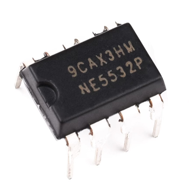 |
NE5532 | Bipolar | 9 | 10 | 5 | Better noise and gain, but draws more power | DIP-8, SOIC-8 |
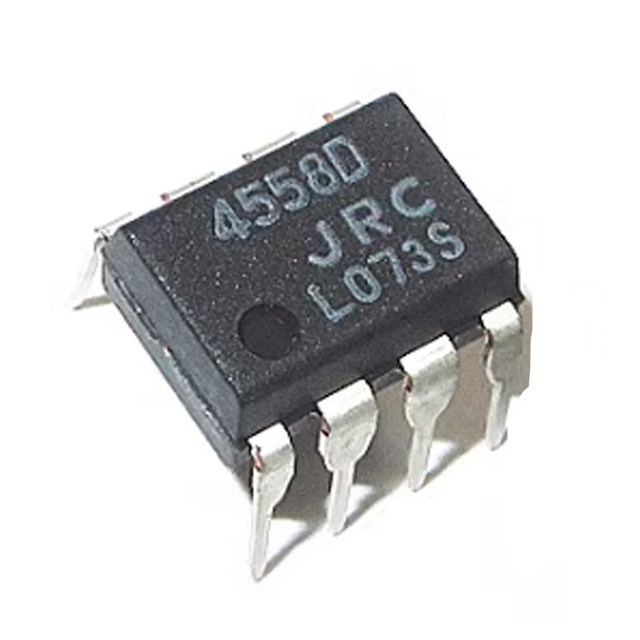 |
JRC4558D | Bipolar | 1.7 | 3 | 8 | Common in tone control/audio EQ; slower than TL072 | DIP-8, SOIC-8 |
Tip:
If your project is audio-related, the OPA2134 is highly recommended for its superior fidelity. For general-purpose signal amplification, TL082 and LF353 offer reliable, cost-effective performance.
TL072 Replacement
These models differ in architecture or parameters but can be used in similar roles depending on the circuit’s needs (e.g., low-voltage operation, power efficiency, precision).
| Picture | Model | Input Type | Slew Rate (V/μs) | GBW (MHz) | Operating Voltage | Key Differences from TL072 | Package Type(s) |
|---|---|---|---|---|---|---|---|
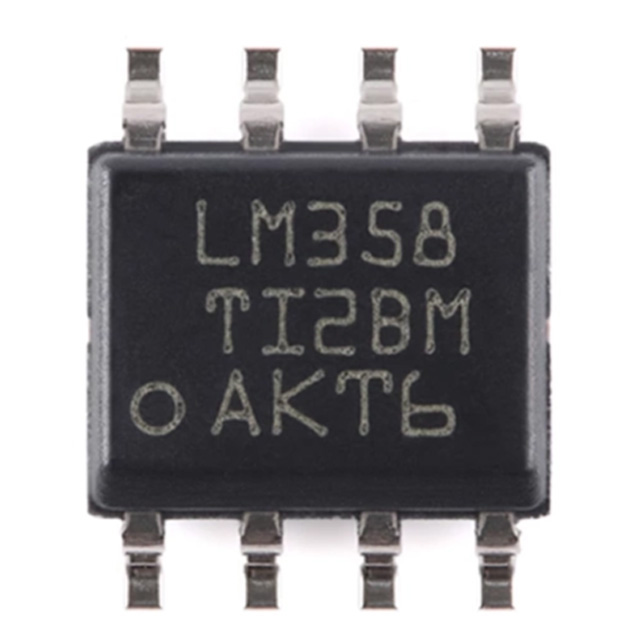 |
LM358 | Bipolar | 0.3 | 1 | 3V–32V | Much slower, lower input impedance; for basic op-amp use | DIP-8, SOIC-8, SOT-23-8 |
 |
MCP602 | CMOS | 7 | 10 | 2.5V–5.5V | CMOS input, low power, ideal for battery-powered circuits | DIP-8, SOIC-8, MSOP-8 |
 |
LM324 | Bipolar | 0.5 | 1 | 3V–32V | Quad op-amp, limited bandwidth, low slew rate | DIP-14, SOIC-14 |
 |
AD712 | Bipolar | 0.3 | 1 | ±3V to ±18V | High-precision amplifier; slower but ultra-stable | DIP-8, SOIC-8 |
 |
NJM2068 | Bipolar | 6.5 | 6 | ±3V to ±18V | Low distortion audio op-amp with better THD specs | DIP-8, SOIC-8 |
Tip:
LM358 and LM324 are great for cost-sensitive, low-speed control systems.
MCP602 is optimal for 3.3V microcontroller projects.
NJM2068 is a solid upgrade for TL072 in hi-fi applications without much cost increase.
AD712 fits precision analog instrumentation.
TL072 Package Type
To suit different PCB designs, the TL072 comes in several package types:
1. TL072 SOIC (Small Outline Integrated Circuit)
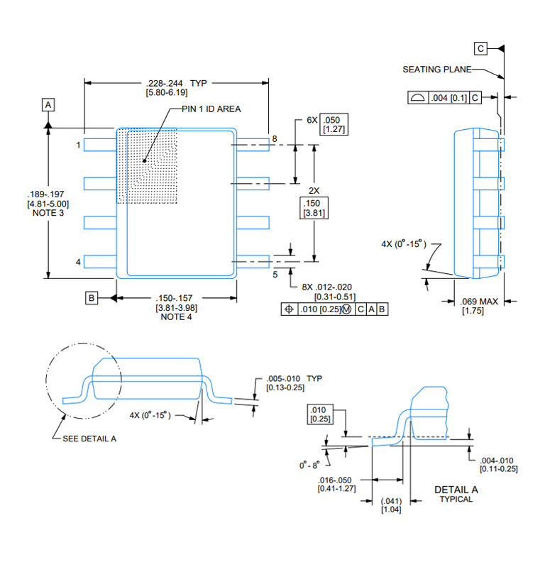
The SOIC version of the TL072 is a standard surface-mount package that includes:
1. 8-pin dual-in-line configuration
2. Gull-wing leads for easy soldering
3. Body widths of 3.9 mm (narrow) or 5.3 mm (wide)
This package is preferred in designs that require a moderate footprint with reliable solder joints. It supports automated assembly processes and provides a good balance between size and heat dissipation. The SOIC format is often selected in scenarios where PCB density is important but not extremely constrained.
2. TL072 SOT (Small Outline Transistor)

In highly space-sensitive layouts, TL072 is offered in SOT-23-5 or SOT-23-6 packages, which are exceptionally compact. These have:
1. Minimal footprint on the PCB
2. Lower power handling due to reduced thermal mass
3. Simplified integration into compact circuit modules
Engineers choose the SOT variant for projects where PCB space is extremely limited, such as miniature sensor boards or ultra-compact analog sections. However, its small size may limit its use in higher power or precision-critical designs without proper thermal consideration.
3. TL072 TSSOP (Thin Shrink Small Outline Package)

The TSSOP version of the TL072 provides a thinner profile and tighter pin pitch than SOIC. It typically features:
1. TSSOP-8 pin configuration
2. Reduced height for slim enclosures
3. Efficient use of PCB real estate
This packaging format is well suited for high-density multilayer PCBs and precision analog sections where vertical clearance is constrained. It allows designers to maintain analog performance while minimizing board area, which is essential in modern compact systems and modular design architectures.
Each TL072 package format gives circuit designers options based on the project’s layout constraints, cooling strategy, and production method—whether it’s optimizing for automated pick-and-place assembly, minimizing footprint, or accommodating enclosure dimensions.
TL072 CAD Model

The TL072 CAD model provides a detailed 3D and footprint representation of the IC, specifically designed for use in PCB layout and circuit simulation environments. It accurately reflects the physical dimensions, pin configuration, and package type—commonly the 8-pin Dual In-line Package (DIP).
These CAD resources typically include:
1. SPICE simulation models for analog performance testing
2. Schematic symbols for integration into circuit diagrams
3. PCB footprints to ensure proper pad alignment and board spacing
Using the TL072 CAD model allows engineers to optimize board layout, prevent mechanical interference, and validate signal routing during the design phase. It also supports compatibility with major EDA tools like KiCad, Eagle, Altium Designer, and OrCAD, enhancing the overall efficiency of both prototyping and production workflows.
Conclusion
The TL072 op amp continues to be a reliable, high-performance choice for analog designers. Thanks to its low noise, fast slew rate, and JFET input stage, it excels in audio, signal conditioning, and instrumentation systems.
Its wide adoption, long-term availability, and array of equivalents and replacements ensure that the TL072 will remain a cornerstone in analog circuit design for years to come—whether you’re working on a high-end preamp or a low-cost buffer.
Please send RFQ , we will respond immediately.
Frequently Asked Questions
1. What is the price of the TL072 op amp?
The price of the TL072 op amp varies depending on the retailer and the quantity purchased. On average, the single-unit price for the TL072 typically ranges from $0.30 to $1.00 USD.
2. Where can I find the TL072 datasheet?
You can find the TL072 op amp datasheet on our official website
3. What information is included in the TL072 datasheet?
The TL072 datasheet contains essential information such as pinout diagrams, electrical characteristics, typical application circuits, package types, and operating conditions.
4. Can the TL072 be used in high-speed applications?
The TL072 has a typical slew rate of 13 V/µs, which allows it to handle moderate-speed signals. However, for high-speed applications requiring faster response times, op-amps with higher slew rates may be more appropriate.