
LNK564PN pinout | circuit diagram | datasheet
- Изоляция выхода: Изолированный
- Топология: Обратный полет
- Защита от неисправностей: Ограничение тока, разомкнутый контур, перегрев, короткое замыкание
- Упаковка: 8-ПДИП-Б


БЕСПЛАТНАЯ доставка для заказов свыше HK$250.00

Быстрый ответ, быстрая расценка

Быстрая отправка, никаких проблем после продажи

Оригинальный канал, гарантия подлинности продукции
{276} LNK564PN, Datasheet, Application Circuit Diagram, Equivalent, for LNK562, LNK563 & LNK564 Urdu
LNK564PN Circuit Diagram
LNK564PN is an integrated IC commonly used in low-power flyback switching power supply designs, with low cost, low power consumption, high efficiency, and few external components. In this article, we will introduce the principle and structure of low-power integrated switching power supply ICs LNK564PN
1、LNK564PN Principle
LNK564PN is a controller switch IC that provides up to 3 W of output power due to its cost-effective alternative to power supplies based on unregulated isolated linear transformers (50/60 Hz). It is a design based on a single common input instead of multiple linear transformers. The self-made bias circuit outputs very low no-load power consumption of 150 mW. Internal oscillator frequency jitter to the symbol Fi does not reduce the quasi-peak sum
Average EMI, optimize filter cost
2. LNK564PN Internal structure circuitry
The internal structure of the chip consists of a 700 V power MOSFET switch and a power controller. Unlike traditional PWM (Pulse Width Modulation) controllers, it uses simple ON/OFF control to regulate the output voltage. The controller consists of an oscillator, feedback (sensing and logic) circuitry, a 5.8 V regulator, BP pin undervoltage circuitry, overtemperature protection, frequency jitter, current limiting circuitry, and leading-edge blanking. The compact structure facilitates PCB layout and routing, as shown in the figure LNK564PN Functional Block Diagram
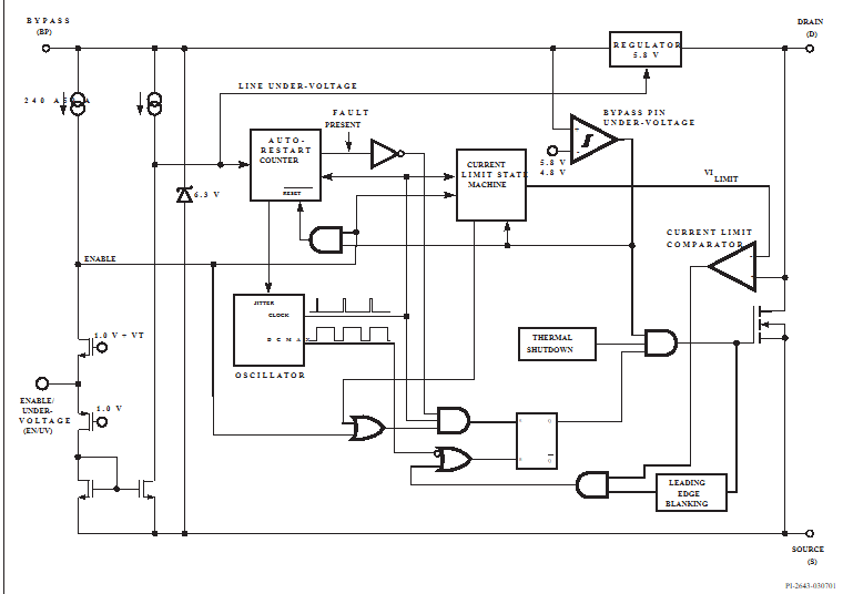
LNK564PN Internal Circuit Diagram
3. Classical circuit analysis
Input stage: BR1 rectifier bridge + C/L filtering
Transformer: E-type core, the ratio of turns of secondary to bias winding determines the output voltage of 25V.
Output stage: secondary rectifier diode (e.g., 1N4007) + filter capacitor (e.g., 470μF) 24V.
Feedback network: Resistor divider (R1/R2) or Zener diode (VR) connected to FB pin
LNK564PN the advantages of high efficiency, low cost, small number of components, high parameter accuracy, and use proprietary IC fine-tuning technology and transformer structure technology; Precise parameter tolerances enable clamping design, reduce costs and improve efficiency; Meets the industry standard requirements for thermal overload protection, hysteresis thermal shutdown protection and auto-recovery to prevent overheating damage improves field reliability, low-cost input filtering configuration, and the IC enters auto-restart mode when the output is short-circuited or open-loop, limiting the output power to ≥85% of normal.

LNK564DN Classic circuitry
Больше похожего

74HCT08PW
Нексерия

74AHC1G02GV
Нексерия

CD4081BF3A
Техасские инструменты
74AHCT1G00GW
Нексерия
74AHCT1G08GW
Нексерия
TC4001BP
Тошиба
CD4011BF3A
Техасские инструменты
74AHCT14PW
Нексерия
TC7S02FU
Тошиба

74LVC00AD
Нексерия
74HC10D
Нексерия
74AHCT541PW
Нексерия
Также добавить в корзину

MAX828EUK+T
Analog Devices Inc./Maxim Integrated
DS28CM00R-A00+T
Analog Devices Inc./Maxim Integrated

MAX3232CSE+T
Analog Devices Inc./Maxim Integrated

AD8515ARTZ
УМВ

SY8502FCC
Силерджи Корпорейшн

LPC2387FBD100K
NXP USA Inc.

LM4040BIM3X-2.5
Национальный полупроводник

RT9610BZQW
Richtek USA Inc.

TCA9543APWR
Техасские инструменты

AMS1086CD-3.3
Современные монолитные системы

LMC6482AIMX/NOPB
Техасские инструменты

ULN2003AD
Техасские инструменты
Сопутствующие товары
74HCT08PW
Нексерия
74AHC1G02GV
Нексерия
CD4081BF3A
Техасские инструменты
74AHCT1G00GW
Нексерия
74AHCT1G08GW
Нексерия
TC4001BP
Тошиба
CD4011BF3A
Техасские инструменты
74AHCT14PW
Нексерия
TC7S02FU
Тошиба
74LVC00AD
Нексерия
74HC10D
Нексерия
74AHCT541PW
Нексерия
74HC132PW
Нексерия
74HC1G04GV
Нексерия
74AHC1G04GW
Нексерия
74AHC1GU04GW
Нексерия
74HC27D
Нексерия
TC7S00FU
Тошиба
74LVC00APW
Нексерия
74HCT86D
Нексерия
74LVC1G11GW
Нексерия
HEF4071BT
Нексерия

74LVC1G02GV
Нексерия
HEF4070BT
Нексерия

MC14093BCP
онсеми
74HC32PW
Нексерия
74HC1G08GW
Нексерия
74AHC00D
Нексерия
74LVC1G86GW
Нексерия

HEF4093BP
NXP Полупроводники
Пожалуйста, отправьте запрос предложения, мы ответим немедленно.
