
CD4001BE pinout, application & circuit
- Тип логики: NOR Gate
- Количество цепей: 4
- Количество входов: 2
- Упаковка: 14-ПДИП


БЕСПЛАТНАЯ доставка для заказов свыше HK$250.00

Быстрый ответ, быстрая расценка

Быстрая отправка, никаких проблем после продажи

Оригинальный канал, гарантия подлинности продукции
CD4001BE Pinout
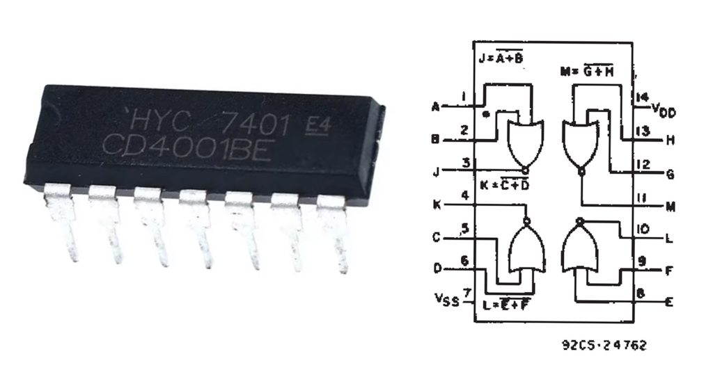
The CD4001BE is a CMOS integrated circuit that contains four independent 2-input NOR gates. This versatile IC is commonly used in digital logic circuits for performing logical operations. Each NOR gate provides an output that is the inverse of the logical OR operation between its two inputs. The CD4001BE is designed to be reliable in a wide range of electronic applications, offering both high noise immunity and low power consumption. It is available in a 14-pin package, with each pin having a specific function that is critical for proper operation.
| Номер контакта | Pin Description | Detailed Description |
|---|---|---|
| 1 | Input A (First NOR Gate) | This is the first input for the first NOR gate. A logical signal is applied here. |
| 2 | Input B (First NOR Gate) | This is the second input for the first NOR gate. A logical signal is applied here. |
| 3 | Output J (First NOR Gate) | The output of the first NOR gate. This is the result of the logical NOR operation between inputs A and B. |
| 4 | Input C (Second NOR Gate) | This is the first input for the second NOR gate. A logical signal is applied here. |
| 5 | Input D (Second NOR Gate) | This is the second input for the second NOR gate. A logical signal is applied here. |
| 6 | Output K (Second NOR Gate) | The output of the second NOR gate. This is the result of the logical NOR operation between inputs C and D. |
| 7 | Ground (Vss) | The ground pin, typically connected to the negative side of the power supply (0V or GND). |
| 8 | Input E (Third NOR Gate) | This is the first input for the third NOR gate. A logical signal is applied here. |
| 9 | Input F (Third NOR Gate) | This is the second input for the third NOR gate. A logical signal is applied here. |
| 10 | Output L (Third NOR Gate) | The output of the third NOR gate. This is the result of the logical NOR operation between inputs E and F. |
| 11 | Input G (Fourth NOR Gate) | This is the first input for the fourth NOR gate. A logical signal is applied here. |
| 12 | Input H (Fourth NOR Gate) | This is the second input for the fourth NOR gate. A logical signal is applied here. |
| 13 | Output M (Fourth NOR Gate) | The output of the fourth NOR gate. This is the result of the logical NOR operation between inputs G and H. |
| 14 | Vcc (Power Supply) | The power supply pin, typically connected to the positive voltage source (e.g., +5V or +12V). |
The pinout of the CD4001BE integrated circuit includes a variety of input, output, and power connections, all of which are carefully arranged to support the four independent NOR gates. From feeding logic signals to the gates to providing the necessary power and ground connections, each pin plays a critical role in the function of the integrated circuit. Understanding the pin layout and the function of each pin is key to using the IC effectively in logic circuits and other applications that require logic operations.
Больше похожего

ISL91212BIIZ-TR5928
Ренесас / Интерсил
LM26484SQ
Техасские инструменты

TLE9262QX
Технологии Инфинеон

LTC1473CGN
Аналоговые Устройства
ACT8846QM468
Корво

LTC4357MPMS8
Аналоговые Устройства

LTC1923EUH
Аналоговые Устройства

LTC4354IDDB
Аналоговые Устройства
DA6011-02HDA2
Ренесас / Диалог

LTC4413EDD
Аналоговые Устройства

LTC4412HVIS6
Аналоговые Устройства

LTC1923EGN
Аналоговые Устройства
Также добавить в корзину
.jpg "LM2674M-5.0")
LM2674M-5.0
Техасские инструменты
,TO-226_straightlead.jpg "TL431ACZ")
TL431ACZ
онсеми

ADG1408YCPZ-REEL7
Аналоговые Устройства Inc.

LMC6482IMX/NOPB
Техасские инструменты

STM32F429VET6
STMicroelectronics

MT40A1G16KD-062E:E
Микрон Текнолоджи Инк.

SN74LVC2G125YZPR
Техасские инструменты

BQ24314DSGR
Техасские инструменты

TL431AIL3T
STMicroelectronics

TMS320C6713BZDP300
Техасские инструменты
SCM1242MF
Sanken Electric USA Inc.

XL4003E1
XLSEMI
Сопутствующие товары
ISL91212BIIZ-TR5928
Ренесас / Интерсил
LM26484SQ
Техасские инструменты
TLE9262QX
Технологии Инфинеон
LTC1473CGN
Аналоговые Устройства
ACT8846QM468
Корво
LTC4357MPMS8
Аналоговые Устройства
LTC1923EUH
Аналоговые Устройства
LTC4354IDDB
Аналоговые Устройства
DA6011-02HDA2
Ренесас / Диалог
LTC4413EDD
Аналоговые Устройства
LTC4412HVIS6
Аналоговые Устройства
LTC1923EGN
Аналоговые Устройства

SY8370C1TMC
Силергия
TLE9263QX
Технологии Инфинеон

AXP803
ООО «ОЛИМЕКС»

LTC1968IMS8
Аналоговые Устройства
LP2998MAX
Техасские инструменты
TLE9262-3QX
Технологии Инфинеон
ACT8846QM490
Корво

LTC4411ES5
Аналоговые Устройства
LTC1967CMS8
Аналоговые Устройства
TLE9262BQX
Технологии Инфинеон

AXP209
ООО «ОЛИМЕКС»
P91E0A-I5NHGI
Ренесас Электроникс
P91E0A-I5NHGI8
Ренесас Электроникс
LM26480SQ-AA
Техасские инструменты
TLE9263-3BQX
Технологии Инфинеон
LTC1968CMS8
Аналоговые Устройства
TLE9263BQX
Технологии Инфинеон
TEA1716T/2
NXP Полупроводники
Пожалуйста, отправьте запрос предложения, мы ответим немедленно.
