
TIP41C Transistor | Datasheet | Pinout | Amplifier Circuit onsemi
- Transistor Type: NPN
- Current-Collector(Ic)(Max): 6 A
- Voltage-Collector Emitter Breakdown (Max): 100 V
- Package: TO-220-3


FREE delivery for orders over HK$250.00

Quick response, quick quotaton

Flash shipment,no worries after sales

Original channel,guarantee of the authentic products
TIP41C TIP42C Amplifier Circuit | DIY Audio Amplifier using Transistors
TIP41C Pinout
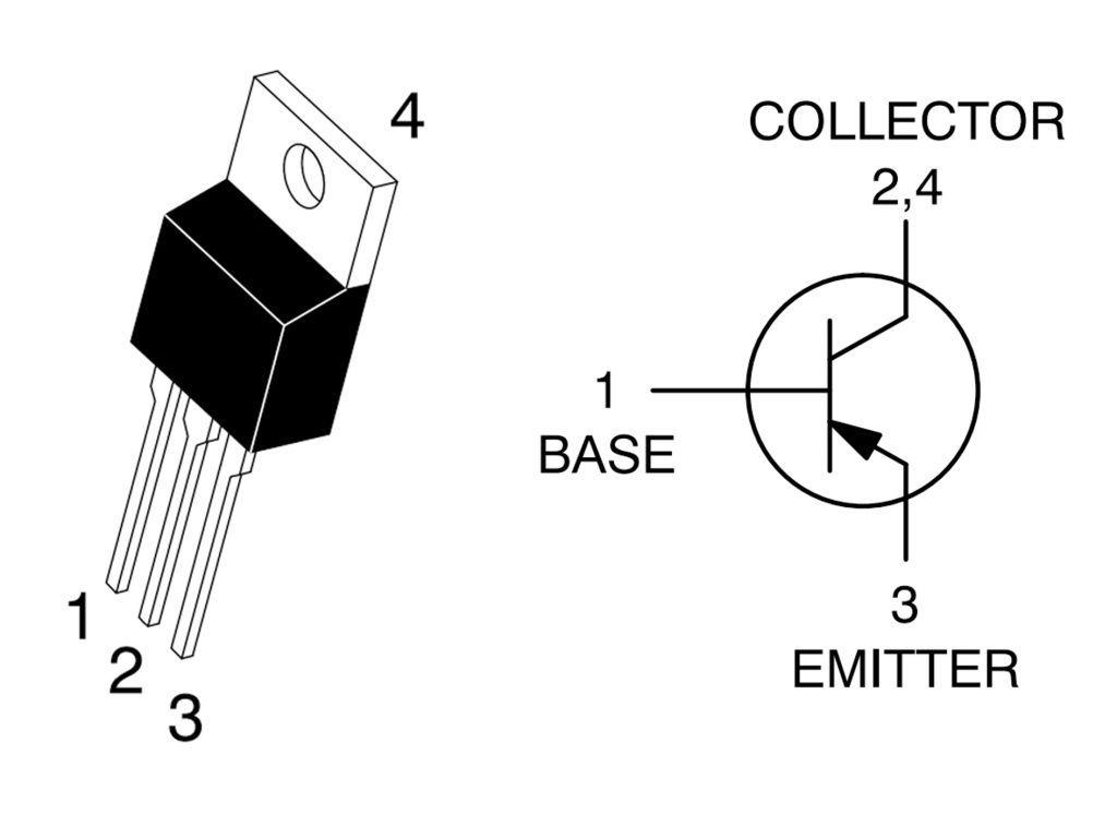
TIP41C Pinout Diagram
The TIP41C is an NPN power transistor commonly used in various electronic applications, particularly in amplifiers and switching circuits. The following table outlines the pinout configuration and the corresponding descriptions for each pin of the TIP41C.
| Pin Number | Pin Name | Description |
|---|---|---|
| 1 | Base | The base pin controls the current flow between the collector and emitter. It is used to turn the transistor on and off. |
| 2, 4 | Collector | The collector pins are where the current enters the transistor from the load, and they are connected to the power supply. |
| 3 | Emitter | The emitter pin is where the current leaves the transistor to flow to ground. |
The above pinout information provides an overview of the key functions of the TIP41C transistor’s pins. Understanding this configuration is essential for proper usage in electronic circuits, ensuring correct placement of the base, collector, and emitter connections for optimal performance.
Tip41C Amplifier Circuit
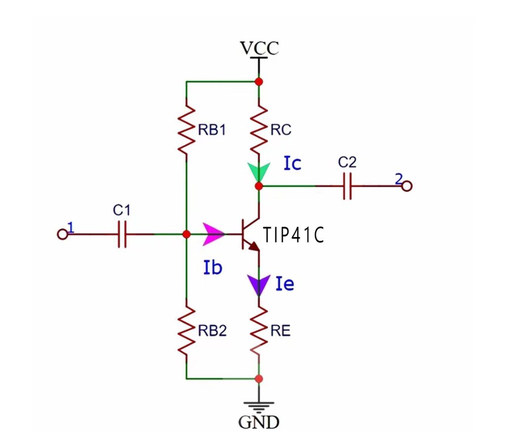
Tip41C Amplifier Circuit Diagram
The TIP41C is an NPN power transistor commonly used in various types of amplifiers. It features high power handling capability and low saturation voltage, making it ideal for many electronic projects. The following is a typical design description of the TIP41C amplifier circuit.
Input Stage:
The AC signal is fed into the base of the TIP41C through a coupling capacitor (e.g., 10µF). The capacitor ensures that only the AC part of the signal passes through, blocking any DC offset.
Base Biasing:
1. A resistor (typically in the range of 10kΩ to 100kΩ) is connected between the base of the transistor and a positive DC voltage supply to properly bias the transistor into the active region.
2. A voltage divider network (comprising two resistors) can also be used to set a stable operating point for the transistor.
Collector Load:
The collector is connected to the positive voltage supply (Vcc) through a collector resistor (e.g., 1kΩ). This resistor determines the gain of the amplifier.
Emitter Stabilization:
1. A resistor (typically 100Ω to 1kΩ) is placed in series with the emitter to stabilize the operating point and prevent thermal runaway.
2. An optional emitter bypass capacitor (e.g., 100µF) may be placed across the emitter resistor to improve the amplifier’s frequency response, especially at higher frequencies.
Output Stage:
The amplified signal is taken from the collector of the TIP41C. This output is often passed through a coupling capacitor (e.g., 10µF) to remove any DC component before sending it to the next stage or speaker.
Power Supply:
The circuit requires a DC power supply that provides an appropriate voltage (e.g., 12V to 24V) for the amplifier to operate effectively.
Working Principle
1. Input Voltage: The input voltage is fed into the circuit, where it will be controlled by the potentiometer. The potentiometer adjusts the level of the input voltage to the base of the TIP41C transistor, which then allows the transistor to amplify the signal.
2. Amplification Process: As the potentiometer adjusts, it modulates the base current flowing into the TIP41C. Since the TIP41C is a power transistor, it uses this small current to control a larger current flow from the collector to the emitter, thereby amplifying the input signal.
3. Output Voltage: The output voltage varies depending on the potentiometer setting. The circuit is designed to output a voltage range from 0V to 60V, allowing for flexibility in control. The output could be used to power a load or another stage in a system.
More Like This

MMBT5550LT1G
onsemi

MMBT2222A
HY Electronic (Cayman) Limited
MMBT3904
HY Electronic (Cayman) Limited
MMBT2907A
HY Electronic (Cayman) Limited

TIP41C
Fairchild Semiconductor

PMBT3904,215
NXP Semiconductors

TIP120
Central Semiconductor Corp

TIP36C
Central Semiconductor Corp
TIP35C
Central Semiconductor Corp

TIP3055
Central Semiconductor Corp
TIP2955
Central Semiconductor Corp
TIP147
Central Semiconductor Corp
Also Add to Cart

NJD2873T4G
onsemi
TIP127
STMicroelectronics

2SC1623
MDD

2N3773
Microchip Technology
TIP31C
onsemi
,TO-226_straightlead.jpg "ZTX651")
ZTX651
Diodes Incorporated

BC817-40,215
Nexperia USA Inc.

MJH6284G
onsemi

SMMBT3904LT1G
onsemi
TIP142
onsemi
D44H11
STMicroelectronics

2N2222A
STMicroelectronics
Related Products
MMBT5550LT1G
onsemi
MMBT2222A
HY Electronic (Cayman) Limited
MMBT3904
HY Electronic (Cayman) Limited
MMBT2907A
HY Electronic (Cayman) Limited
TIP41C
Fairchild Semiconductor
PMBT3904,215
NXP Semiconductors
TIP120
Central Semiconductor Corp
TIP36C
Central Semiconductor Corp
TIP35C
Central Semiconductor Corp
TIP3055
Central Semiconductor Corp
TIP2955
Central Semiconductor Corp
TIP147
Central Semiconductor Corp
TIP142
Central Semiconductor Corp
2N2369AUB
Microchip Technology

BCX17
onsemi

BCP69
onsemi
BCP53
onsemi
PZT2907A
onsemi

2SC5200
STMicroelectronics

2N2907A
Micro Commercial Co

BCP52-16
STMicroelectronics

MMBTA92
STMicroelectronics

2N3773
STMicroelectronics
2N5551
onsemi
MPSA92
onsemi
MPS751G
onsemi
MJD44H11
onsemi
MJD127
onsemi

2SC4617
onsemi
TIP42C
onsemi
Please send RFQ , we will respond immediately.
