When you’re hooking up your TFP401APZP chip with an FPGA, here’s what you need to know for a smooth setup. First off, connect your HDMI’s TMDS signals to the TFP401APZP pins—RXC± handles the clock, while RX0±, RX1±, and RX2± manage the data channels. Don’t forget to use 0.1μF AC coupling capacitors on each pair of differential lines; it keeps your signals clean.

TFP401APZP datasheet & pdf
Explore the TFP401APZP Reference Manual for comprehensive technical details and specifications. This PDF document provides essential information, supporting your efforts to enhance your projects with the TFP401APZP component.
- Type: Receiver
- Protocol: -
- Number of Drivers/Receivers: -
- Package: 100-TQFP Exposed Pad


FREE delivery for orders over HK$250.00

Quick response, quick quotaton

Flash shipment,no worries after sales

Original channel,guarantee of the authentic products
TFP401APZP
Let me tell you a bit about the TFP401APZP chip. If you’re designing anything that involves video signals, this one’s pretty handy. It supports a single-link TMDS interface and fully complies with the DVI 1.0 standard. That means it can easily handle pixel clock frequencies up to 165MHz, giving you crisp resolutions as high as 1920×1200.
Inside, it has a built-in TMDS receiver and decoder that outputs clear, 24-bit true-color RGB data. Plus, it has hot-plug detection and automatic synchronization, which really boosts compatibility with various devices. And because it runs at low power, it’s ideal for portable gadgets or battery-sensitive applications.
Finally, it comes in a compact 100-pin TQFP package (PZP), making your PCB layout neat and integration smoother.
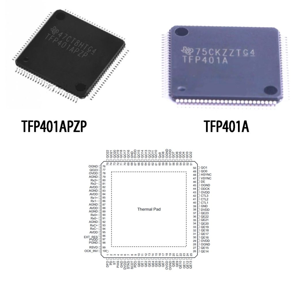
TFP401APZP Pinout Diagram

| Pin Number | Pin Name | Type | Description |
|---|---|---|---|
| 2 | PD | DI | Power-down control, low logic level to enter low power mode, high logic level to enter normal mode. |
| 4 | PIXS | DI | Signal input for controlling the system’s mode, low logic level enters the standby mode, high logic level enters the normal mode. |
| 7 | STAG | DI | Stage input for system control. Enter a specific stage when triggered by the controller. |
| 8 | SCDT | DO | Signal output for data status feedback, indicating the current status. |
| 9 | PDO | DI | Data output pin for transmitting processed information. |
| 10-17 | QEO-QE7 | DO | Output signals, varying depending on system configuration. |
| 20-27 | QEB-QE15 | DO | Output signals, varying depending on system configuration. |
| 30-37 | QE16-QE23 | DO | Output signals, varying depending on system configuration. |
| 49-56 | QOO-QO7 | DO | Feedback signals from the system. (Only valid when the system is in a specific state.) |
| 59-66 | QO8-QO15 | DO | Feedback signals from the system. (Only valid when the system is in a specific state.) |
| 69-75,77 | QO16-QO23 | DO | Feedback signals from the system. (Only valid when the system is in a specific state.) |
| 44 | ODCK | DO | Output data clock signal for system control during data exchange. |
| 80,81 | Rx2± | AI | TMDS signal input (Red data). |
| 85,86 | Rx1± | AI | TMDS signal input (Green data). |
| 90,91 | RxC± | AI | TMDS signal input (Blue data). |
| 93,94 | RxC± | AI | TMDS signal input (Blue data). |
| 97 | PVDD | VDD | Internal PLL power supply. |
| 98 | PGND | GND | Internal PLL ground. |
| 18,29,43,57,78 | OVDD | VDD | Output voltage power supply. |
| 1,19,28,38,45,58,76,79,96,100 | GND | GND | Ground. |
When you’re using the TFP401APZP chip, you’ll want to pay attention to pin functions to keep your design stable. The PD pin manages the chip’s overall power state—pull it low to enter a low-power mode—while the PDO pin controls the output drivers, setting most outputs to high impedance if it’s low. PIXS selects your pixel mode, and STAG helps control pixel interleaving to reduce noise. SCDT confirms you’ve got a valid sync signal. TMDS inputs Rx0±, Rx1±, Rx2±, and RxC± handle blue, green, red, and clock signals. QE and QO pins output image data based on your chosen mode. Keep these guidelines in mind for smooth operation.
TFP401APZP Hdmi To Rgb Circuit & TFP401APZP Schematic For Video Decoder

When you’re dealing with HDMI signals using the TFP401APZP chip, here’s how things typically work: First, your HDMI signals enter through differential inputs (like RxC±, Rx0±, Rx1±, Rx2±). Inside the chip, these signals get buffered and decoded from the TMDS serial format into parallel 24-bit RGB data. Alongside RGB, you’ll also get synchronization signals—HSYNC, VSYNC, and DEN—coming out from dedicated output pins. These outputs let you directly drive external displays such as LCD panels or other RGB modules. To keep everything synchronized, the chip uses an external 28.6363 MHz crystal oscillator as a stable clock source. And don’t forget, this chip needs different voltage levels—typically 1.8V and 3.3V—supplied through the DVDD (digital) and IVDD (analog internal) power pins, making sure each part inside the chip works correctly and smoothly.、
TFP401APZP Ti Hdmi Dvi Receiver & TFP401APZP To Lcd Panel Interface
Let’s say you’re building your own custom HD display, maybe for a Raspberry Pi, industrial control board, or some embedded multimedia system. You’ll likely need to convert HDMI signals into TTL RGB signals that your TFT LCD panel can actually use—and that’s where the TI TFP401APZP chip steps in to help.
Imagine you’re expanding the display capabilities of a Raspberry Pi or adding touchscreen functionality to industrial equipment. First, you’ll connect your HDMI source—such as a PC or Raspberry Pi—to receive TMDS differential signals (clock and RGB data) via standard HDMI input. These signals then pass through 0.1μF AC coupling capacitors directly to the TFP401APZP’s differential inputs (RXC±, RX0±, RX1±, RX2±). Inside the chip, all the complex signal decoding gets done automatically, turning TMDS signals into clear 24-bit RGB data, along with sync signals (HSYNC, VSYNC) and data enable signals (DEN). Finally, you feed these signals straight to your LCD panel, creating an easy, stable HD video solution.
TFP401APZP Edid Configuration Example

Here’s how you can set up an EDID configuration circuit using the TFP401AZP chip paired with a 24LC02 EEPROM. This circuit helps your HDMI device, like a PC or Raspberry Pi, automatically configure video signals by reading stored EDID data.
You’ll start by powering both the TFP401AZP and 24LC02 with a stable 3.3V supply. Don’t forget to include two 4.7kΩ pull-up resistors on the I²C lines (SCL, SDA) for reliable data communication. Your HDMI interface’s DDC clock and data lines should directly connect to the TFP401AZP and EEPROM’s respective SCL and SDA pins, letting your HDMI source easily access EDID info.
With all address pins (A0, A1, A2) grounded, your EEPROM’s address becomes the standard 0x50. The WP (write-protect) pin is controlled by TFP401AZP, protecting your EDID settings from accidental changes.
Once connected, your HDMI source reads EDID from the EEPROM, automatically configuring video signals that the TFP401AZP decodes into RGB, powering your external TFT LCD perfectly.
TFP401APZP vs TFP401A Performance
| Parameter | TFP401APZP | TFP401A |
|---|---|---|
| Function Description | HDMI/DVI receiver (without HDCP) | HDMI/DVI receiver (without HDCP), includes HSYNC jitter suppression |
| Maximum Pixel Clock | 165 MHz | 165 MHz |
| Maximum Supported Resolution | 1920×1200@60Hz (WUXGA) | 1920×1200@60Hz (WUXGA) |
| Input Signal Type | TMDS differential signal | TMDS differential signal |
| Output Interface Type | 24-bit RGB Parallel (TTL) | 24-bit RGB Parallel (TTL) |
| HSYNC Jitter Correction | None | Yes (Integrated HSYNC regeneration, enhanced jitter tolerance) |
| Output Clock Jitter Performance | Standard Performance | Superior (Suitable for applications requiring high timing accuracy) |
| Package Type | 100-pin TQFP | 100-pin TQFP |
| Power Supply Requirements | 3.3V, 1.8V | 3.3V, 1.8V |
| Application Scenario | General video display conversion applications | Applications demanding high timing precision |
Looking at the table above, you’ll notice the TFP401APZP and TFP401A chips are almost identical in terms of overall performance and packaging. But the biggest difference comes down to how they handle HSYNC jitter. The TFP401A has a built-in HSYNC regeneration circuit, making its output signals significantly more stable.
So here’s my suggestion: If you’re working in an environment with good signal quality, and your project doesn’t demand ultra-stable video synchronization, then the TFP401APZP is perfectly fine—and it’ll probably save you some money.
However, if your application involves precision displays—like those used in high-end industrial systems, medical equipment, or professional-grade monitors—then you’ll want to opt for the TFP401A. Its HSYNC jitter correction ensures top-notch display quality and system reliability.
Always consider your specific HSYNC stability needs and cost factors carefully, and choose the chip that best fits your project requirements.
TFP401APZP Rgb Output Wiring
If you’re wiring the TFP401APZP chip to an LCD display, here’s exactly how you’d do it. First, you’ll deal with the RGB signals, which come in three separate 8-bit channels: connect pins 83–90 for red, 91–98 for green, and 99–106 for blue directly to your LCD’s RGB inputs.
Next up, you’ll handle sync signals to ensure everything stays timed right. Connect HSYNC (pin 107), VSYNC (pin 108), DE (data enable, pin 109), and ODCK (data clock, pin 110) straight to your LCD’s matching input pins.
You’ll also have some configuration pins to adjust how your chip works: PIXS decides whether you output one pixel per clock (low) or two pixels per clock (high). OCK_INV flips your clock polarity if needed, and the ST pin sets the drive strength—go high for stronger signals or low if you don’t need the extra strength.
Make sure to power your chip correctly: DVDD needs 1.8V, while AVDD and PVDD require 3.3V each. Use proper decoupling capacitors right next to these pins to keep noise down.
And if your system needs EDID information, just hook up an EEPROM like the 24LC02 chip to your DDC lines: pin 111 (SCL) and pin 112 (SDA). This lets your HDMI source easily detect your display’s capabilities automatically.
TFP401APZP Display Interface Ic
If you’re looking to convert HDMI or DVI signals into parallel RGB for your TFT LCD panels, the TFP401APZP chip can make things easy for you—perfect for DIY LCD displays or custom setups. It’s also great if you’re working with digital projectors, ensuring you get crystal-clear, stable images even at high resolutions. For those involved in embedded systems—think industrial controls, medical devices, or anywhere high-quality visuals really count—this chip helps you achieve reliable, professional-grade displays. And if you’re into education tech or presentations, like interactive whiteboards or multimedia classrooms, it’ll give your visuals that extra clarity and stability you need.
TFP401APZP Fpga Hdmi Input
More Like This

74HCT280D,653
NXP USA Inc.

74HCT280N,652
NXP USA Inc.
N74F280BN,602
NXP USA Inc.

1621B2UZZGR
Texas Instruments
1621B1UZZGR
Texas Instruments

SN74S280NSRG4
Texas Instruments

SN74LS280DRG4
Texas Instruments
SN74AS286NSRG4
Texas Instruments
SN74AS286DRG4
Texas Instruments
SN74AS280DRG4
Texas Instruments
SN74ALS280DRG4
Texas Instruments
SN74ALS280DG4
Texas Instruments
Also Add to Cart

DRV8860PWR
Texas Instruments

74HCT165D
Nexperia

STM32G0B1RBT6
STMicroelectronics

TLV271IDBVR
Texas Instruments

SN65HVD1782D
Texas Instruments

SGM61230XTN6G/TR
SGMICRO

LM3409MYX/NOPB
Texas Instruments

TPS628640AYCGR
Texas Instruments

MX25L25635FZ2R-10G
Macronix

MPQ4323GDE-AEC1-Z
Monolithic Power Systems Inc.

ADSP-BF548BBCZ-5A
Analog Devices Inc.

AD9512BCPZ
Analog Devices Inc.
Related Products
74HCT280D,653
NXP USA Inc.
74HCT280N,652
NXP USA Inc.
N74F280BN,602
NXP USA Inc.
1621B2UZZGR
Texas Instruments
1621B1UZZGR
Texas Instruments
SN74S280NSRG4
Texas Instruments
SN74LS280DRG4
Texas Instruments
SN74AS286NSRG4
Texas Instruments
SN74AS286DRG4
Texas Instruments
SN74AS280DRG4
Texas Instruments
SN74ALS280DRG4
Texas Instruments
SN74ALS280DG4
Texas Instruments

CY74FCT480BTSOCTG4
Texas Instruments
CD74AC280M96G4
Texas Instruments
74ACT11286NG4
Texas Instruments
74ACT11286N
Texas Instruments

SY10E193JZ TR
Microchip Technology
SY10E193JZ
Microchip Technology
SY10E160JZ TR
Microchip Technology
SY10E160JZ
Microchip Technology
SY100S360JZ-TR
Microchip Technology
SY100S360JZ
Microchip Technology
SY100E193JZ TR
Microchip Technology
SY100E193JZ
Microchip Technology
SY100E160JZ TR
Microchip Technology
SY100E160JZ
Microchip Technology
SN74S280NSRE4
Texas Instruments
SN74S280NSR
Texas Instruments
SN74LS280DRE4
Texas Instruments
SN74LS280DR
Texas Instruments
Please send RFQ , we will respond immediately.
Please send RFQ , we will respond immediately.
Copyright © 2024 All Rights Reserved