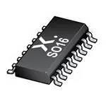
SN74HC164N datasheet, circuit diagram, pinout, pdf
- Logic Type: Shift Register
- Output Type: Push-Pull
- Number of Elements: 1
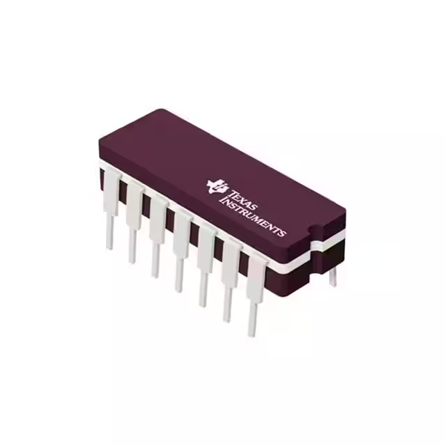
- Package: 14-DIP (0.300, 7.62mm)

FREE delivery for orders over HK$250.00

Quick response, quick quotaton

Flash shipment,no worries after sales

Original channel,guarantee of the authentic products
74HC164N RAIN DROPS CHASER
SN74HC164N Pinout

The SN74HC164N is an 8-bit serial-in, parallel-out shift register IC commonly used in digital circuits for data expansion and display driving. It features dual gated serial data inputs (A and B), a common clock (CLK), and asynchronous clear (CLR) for resetting all outputs. This pinout table provides a detailed reference for all 14 pins of the SN74HC164N, helping ensure proper connectivity in electronic designs.
| Pin No. | Name | I/O | Description |
|---|---|---|---|
| 1 | A | I | Gated Serial Input 1 |
| 2 | B | I | Gated Serial Input 2 |
| 3 | QA | O | Parallel Output |
| 4 | QB | O | Parallel Output |
| 5 | QC | O | Parallel Output |
| 6 | QD | O | Parallel Output |
| 7 | GND | – | Ground |
| 8 | CLK | I | Clock |
| 9 | CLR | I | Clear 1 Active-Low |
| 10 | QE | O | Parallel Output |
| 11 | QF | O | Parallel Output |
| 12 | QG | O | Parallel Output |
| 13 | QH | O | Parallel Output |
| 14 | Vcc | — | Power |
Understanding the SN74HC164N pin configuration is essential for successful implementation in shift register applications. With clearly labeled parallel outputs (QA to QH), power and ground connections, and control inputs, this IC enables efficient serial-to-parallel data conversion in microcontroller and logic-based systems.
SN74HC164N Circuit Diagram

The SN74HC164N is a high-speed 8-bit serial-in, parallel-out shift register ideal for reducing the number of GPIO pins required in applications like LED matrix driving. By using this IC as a deserializer, you can efficiently control multiple LEDs with minimal microcontroller I/O overhead.
To prevent LEDs from turning on before valid data or a proper clock signal is received, a sink MOSFET is incorporated into the design. This ensures accurate LED output and avoids unintended lighting during initialization or data shifting.
Design Requirements for SN74HC164N LED Applications
Clock Signal Integrity:
Make sure that the rising edge of the incoming clock complies with the conditions listed under the Recommended Operating Conditions in the datasheet.
Voltage Compliance:
Always confirm that both input and output voltages stay within the limits specified under the Absolute Maximum Ratings to avoid damage.
Input Thresholds:
Refer to the Recommended Operating Conditions section for detailed input voltage threshold levels.
Timing Parameters:
For precise signal timing and stable operation, refer to the Timing Requirements, TA = 25°C in the device datasheet.
Recommended Operating Conditions
| Parameter | Description | SN74HC164 | Unit |
|---|---|---|---|
| VCC | Supply voltage | 2 – 6 | V |
| VIH | High-level input voltage (VCC = 2 V) | ≥ 1.5 | V |
| High-level input voltage (VCC = 4.5 V) | ≥ 3.15 | V | |
| High-level input voltage (VCC = 6 V) | ≥ 4.2 | V | |
| VIL | Low-level input voltage (VCC = 2 V) | ≤ 0.5 | V |
| Low-level input voltage (VCC = 4.5 V) | ≤ 1.35 | V | |
| Low-level input voltage (VCC = 6 V) | ≤ 1.8 | V | |
| VI | Input voltage | 0 to VCC | V |
| VO | Output voltage | 0 to VCC | V |
| Δt/ΔV | Input rise/fall time (VCC = 2 V) | ≤ 1000 | ns |
| Input rise/fall time (VCC = 4.5 V) | ≤ 500 | ns | |
| Input rise/fall time (VCC = 6 V) | ≤ 400 | ns | |
| TA | Operating free-air temperature | –40 to 125 | °C |
Absolute Maximum Ratings
| Parameter | Description | MIN | MAX | UNITS |
|---|---|---|---|---|
| VCC | Supply voltage | –0.5 | 7 | V |
| IIK | Input clamp current (VI < 0 or VI > VCC) | –20 | 20 | mA |
| IOK | Output clamp current (VO < 0 or VO > VCC) | –20 | 20 | mA |
| IO | Continuous output current (VO = 0 to VCC) | –25 | 25 | mA |
| – | Continuous current through VCC or GND | ±50 | mA | |
| Tstg | Storage temperature | –65 | 150 | °C |
Timing Requirements, TA = 25°C
| PARAMETER | DESCRIPTION | VCC | MIN | NOM | MAX | UNIT |
|---|---|---|---|---|---|---|
| fclock | Clock frequency | 2 V | 6 | MHz | ||
| 4.5 V | 31 | |||||
| 6 V | 36 | |||||
| tw | Pulse duration (CLR low) | 2 V | 100 | ns | ||
| 4.5 V | 20 | |||||
| 6 V | 17 | |||||
| tw | Pulse duration (CLK high or low) | 2 V | 80 | |||
| 4.5 V | 16 | |||||
| 6 V | 14 | |||||
| tsu | Setup time before CLK↑ (Data) | 2 V | 100 | ns | ||
| 4.5 V | 20 | |||||
| 6 V | 17 | |||||
| tsu | Setup time before CLK↑ (CLR inactive) | 2 V | 100 | |||
| 4.5 V | 20 | |||||
| 6 V | 17 | |||||
| th | Hold time, data after CLK↑ | 2 V | 5 | ns | ||
| 4.5 V | 5 | |||||
| 6 V | 5 |
FAQ
1. Is the output current sufficient to drive LEDs directly?
Not directly for high-current LEDs. The SN74HC164N provides limited current (typically ±25 mA max per output), so external drivers or resistors are recommended.
2. What are typical applications of the SN74HC164N?
Common uses include LED matrix driving, key scanning, signal routing, and reducing microcontroller pin usage.
3. Is it TTL or CMOS compatible?
It is CMOS logic but compatible with TTL input levels, making it versatile for mixed-signal environments.
