
SN65HVD233QDRQ1 datasheet | price & pdf
- Type: Transceiver
- Protocol: CANbus
- Number of Drivers/Receivers: 1/1
- Package: 8-SOIC (0.154, 3.90mm Width)


FREE delivery for orders over HK$250.00

Quick response, quick quotaton

Flash shipment,no worries after sales

Original channel,guarantee of the authentic products
SN65HVD233QDRQ1
Looking for a reliable transceiver? This device works with both RS-485 and RS-422 standards, making it perfect for differential data transmission. It’s automotive-grade, built to handle tough environments with a temperature range of -40°C to +125°C.
It’s low power, with minimal quiescent current, so it’s great for power-sensitive applications. Plus, it supports data rates up to 20 Mbps for fast, reliable communication in industrial automation.
It has built-in fail-safe protection to keep it working in tough conditions like bus contention or open circuits, and it offers strong ESD protection for reliability in noisy environments.
With a wide supply range (3.3 V to 5.5 V), it’s versatile for various systems. Plus, short-circuit and thermal protection ensures it stays safe under abnormal conditions. It comes in a compact 8-pin SOIC package, making it ideal for tight spaces.
SN65HVD233QDRQ1 3.3V CAN Transceiver
This transceiver runs on just 3.3 volts, making it perfect if you’re designing low-voltage systems. It’s specifically built for CAN bus communications, which means it’ll help your controllers reliably talk to each other, whether you’re working on automotive or industrial applications.
SN65HVD233QDRQ1 Automotive Grade CAN Chip
If you’re designing electronics for vehicles, reliability matters—a lot. This chip meets automotive standards like AEC-Q100, so it’s built tough enough to handle extreme conditions. It’s durable, dependable, and exactly what you need for automotive projects where failure just isn’t an option.
SN65HVD233QDRQ1 Vehicle Network Applications
This one’s designed specifically for vehicle networks. Whether you’re setting up ECUs, diagnostic equipment, or even infotainment systems, this chip ensures smooth and efficient communication on your CAN bus. It helps keep your data flowing reliably, so everything in your vehicle network runs smoothly.
SN65HVD233QDRQ1 pinout
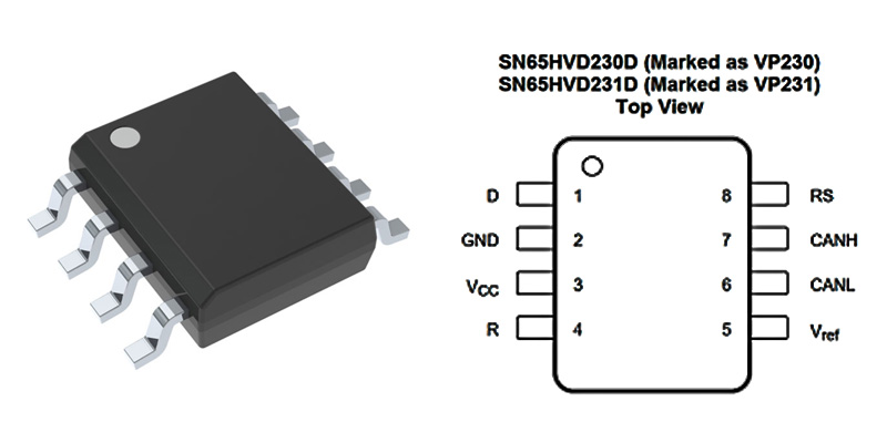
Here is the pinout for the SN65HVD233QDRQ1 in a table format:
| Pin Number | Pin Name | Function |
|---|---|---|
| 1 | A | Non-inverting differential input/output (RS-485) |
| 2 | B | Inverting differential input/output (RS-485) |
| 3 | RO | Receiver Output (logic level) |
| 4 | RE | Receiver Enable (active low) |
| 5 | DE | Driver Enable (active high) |
| 6 | DI | Driver Input (logic level) |
| 7 | GND | Ground |
| 8 | VCC | Supply Voltage (3.3V to 5.5V) |
Important Notes:
Make sure you control the RE and DE pins correctly to switch between transmit and receive modes.
It’s crucial to properly terminate A and B at both the receiver and source ends. If you don’t, signal reflections might occur, which can mess up your data.
RO should only be driven by the differential signals on A and B when the receiver is turned on (RE = low).
Also, always double-check that the voltage supply at VCC is within the recommended range. This is important to avoid any potential damage to your device.
SN65HVD233QDRQ1 Equivalent


SN65HVD233QDRQ1 Equivalent Pinout
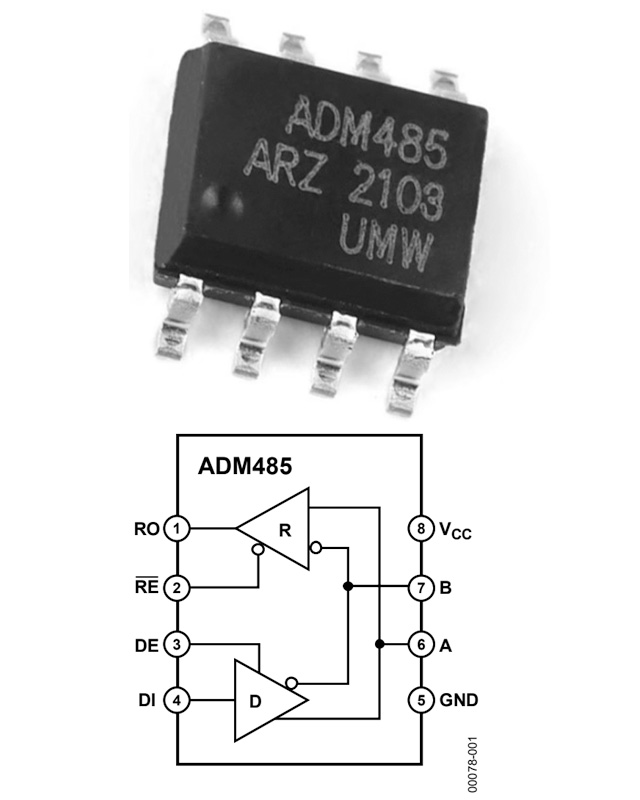
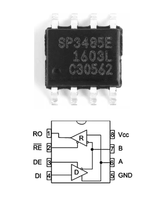
Here is a table comparing the SN65HVD233QDRQ1 with equivalent transceiver models that come in the same 8-pin SOIC package.
| Feature | SN65HVD233QDRQ1 | ADM485ARZ | MAX485CSA | SP3485E |
|---|---|---|---|---|
| Interface | RS-485/RS-422 | RS-485/RS-422 | RS-485/RS-422 | RS-485/RS-422 |
| Data Rate | Up to 20 Mbps | Up to 16 Mbps | Up to 2.5 Mbps | Up to 20 Mbps |
| Supply Voltage | 3.3V to 5.5V | 3.0V to 5.5V | 3.0V to 5.5V | 3.0V to 5.5V |
| Temperature Range | -40°C to +125°C | -40°C to +85°C | -40°C to +85°C | -40°C to +85°C |
| Low Power Consumption | Yes, Low Quiescent Current | Yes, Low Quiescent Current | Yes, Low Quiescent Current | Yes, Low Quiescent Current |
| Driver Enable Pin (DE) | Yes | Yes | Yes | Yes |
| Receiver Enable Pin (RE) | Yes | Yes | Yes | Yes |
| ESD Protection | ±15 kV | ±15 kV | ±15 kV | ±15 kV |
| Package | 8-Pin SOIC | 8-Pin SOIC | 8-Pin SOIC | 8-Pin SOIC |
Summary of Considerations for Replacements:
If you’re working with a device that needs to withstand extreme temperatures, the SN65HVD233QDRQ1 could be the right choice for you. It has a wide temperature range of -40°C to +125°C, making it perfect for automotive and industrial environments. In comparison, the ADM485ARZ, MAX485CSA, and SP3485E only handle temperatures from -40°C to +85°C, so they’re better suited for milder conditions.
When it comes to speed, the SN65HVD233QDRQ1 offers 20 Mbps, which is faster than the ADM485ARZ and MAX485CSA (both support up to 16 Mbps and 2.5 Mbps, respectively). If you need higher communication speeds, go for the SN65HVD233QDRQ1 or SP3485E.
All these devices operate within a 3.0V to 5.5V range, have similar ESD protection, and come in an 8-pin SOIC package, so you can swap them easily in your design.
SN65HVD233QDRQ1 Alternative toTJA1051 CAN Transceiver
Here is a comparison table highlighting the key parameters of the SN65HVD233QDRQ1 and TJA1051 CAN transceivers:
| Feature | SN65HVD233QDRQ1 | TJA1051 |
|---|---|---|
| Interface | RS-485/RS-422 | CAN Bus (Controller Area Network) |
| Data Rate | Up to 20 Mbps | Up to 1 Mbps |
| Supply Voltage | 3.3V to 5.5V | 4.5V to 5.5V |
| Temperature Range | -40°C to +125°C | -40°C to +125°C |
| Low Power Consumption | Yes, Low Quiescent Current | Yes, Low Quiescent Current |
| Receiver Enable Pin (RE) | Yes | Yes |
| Driver Enable Pin (DE) | Yes | No |
| ESD Protection | ±15 kV | ±8 kV |
| Fail-Safe Protection | Yes, integrated protection | Yes, integrated protection |
| Package Type | 8-Pin SOIC | 8-Pin SOIC |
If you’re deciding between the SN65HVD233QDRQ1 and the TJA1051, here’s what you should know. The SN65HVD233QDRQ1 is great for RS-485/RS-422 communication, making it a solid choice for industrial environments. On the other hand, the TJA1051 is built for CAN Bus, which is more specific to automotive and industrial control systems.
When it comes to speed, the SN65HVD233QDRQ1 supports up to 20 Mbps, while the TJA1051 tops out at 1 Mbps. So, if you need faster communication, go with the SN65HVD233QDRQ1.
Both transceivers have similar power requirements and temperature ranges, supporting environments from -40°C to +125°C. The SN65HVD233QDRQ1 also has a Driver Enable (DE) pin, which allows it to switch between transmission and high-impedance states, something the TJA1051 doesn’t offer. Lastly, the SN65HVD233QDRQ1 provides better ESD protection (±15 kV) compared to the TJA1051 (±8 kV), which could be important in noisy settings.
SN65HVD233QDRQ1 CAN Bus Circuit Design

Let me explain a few key points about this CAN bus circuit design to help you better understand how it works.
First, let’s talk about the power supply section. This circuit uses a +3.3V power supply. In the schematic, you’ll notice two ceramic capacitors: one 2.2µF capacitor (C69) and another 100nF capacitor (C73). These capacitors are essential—they filter out noise and interference from the power line, ensuring the chip gets a stable voltage to prevent any issues.
Next, we have the CAN transceiver chip itself, the SN65HVD233QDRQ1. This chip is specifically designed for 3.3V CAN communication and is responsible for transmitting (TXD) and receiving (RXD) signals. Specifically, you’ll connect your CAN transmit signal to the TXD pin, and your received signal comes out of the RXD pin through a 33Ω resistor (R16). This resistor protects the chip from excessive current if the signal becomes abnormal.
There are two more pins on the chip worth noting: the RS pin (pin 8), which is tied directly to ground. This connection places the chip in standard operating mode, minimizing interference during communication. The other is the LBK pin (pin 5), used for loopback testing. The circuit includes a 10kΩ resistor (R145) pulling this pin up to the power supply and a 0Ω resistor (R146) pulling it to ground. This arrangement lets you easily enable or disable loopback mode for debugging or diagnostic purposes.
Finally, let’s look at the CAN bus signal outputs. You’ll see two differential output lines labeled CANH and CANL, which transmit the data signals. The circuit includes two 60.4Ω resistors (R141 and R142) in series, forming a total termination resistance of around 120Ω. This termination is crucial because it reduces signal reflection and enhances stability on the CAN bus.
You’ll also notice a small capacitor of 4700pF (C59), which filters out high-frequency noise, making the signal cleaner. Additionally, there’s a TVS diode labeled NUP2105LT1G. This diode is essential—it protects the CAN bus from sudden voltage spikes or electrostatic discharge, ensuring your chip and the entire CAN bus stay safe and reliable.
More Like This

74HCT280D,653
NXP USA Inc.

74HCT280N,652
NXP USA Inc.
N74F280BN,602
NXP USA Inc.

1621B2UZZGR
Texas Instruments
1621B1UZZGR
Texas Instruments

SN74S280NSRG4
Texas Instruments

SN74LS280DRG4
Texas Instruments
SN74AS286NSRG4
Texas Instruments
SN74AS286DRG4
Texas Instruments
SN74AS280DRG4
Texas Instruments
SN74ALS280DRG4
Texas Instruments
SN74ALS280DG4
Texas Instruments
Also Add to Cart

K4B4G1646E-BMMA
Samsung

HT7833
Holtek Semicon

REF3012AIDBZT
Texas Instruments

NCV8674DS120R4G
onsemi

ADA4932-1YCPZ-R2
Analog Devices Inc.

AMC1311DWV
Texas Instruments
A3950SEUTR-T
Allegro MicroSystems

EMB1499QMHE/NOPB
Texas Instruments

S9KEAZN64AMLC
NXP USA Inc.

TPS56A37RPAR
Texas Instruments

ISL99227BFRZ-TR5782
Renesas Electronics America Inc

F28M35H52C1RFPT
Texas Instruments
Related Products
74HCT280D,653
NXP USA Inc.
74HCT280N,652
NXP USA Inc.
N74F280BN,602
NXP USA Inc.
1621B2UZZGR
Texas Instruments
1621B1UZZGR
Texas Instruments
SN74S280NSRG4
Texas Instruments
SN74LS280DRG4
Texas Instruments
SN74AS286NSRG4
Texas Instruments
SN74AS286DRG4
Texas Instruments
SN74AS280DRG4
Texas Instruments
SN74ALS280DRG4
Texas Instruments
SN74ALS280DG4
Texas Instruments

CY74FCT480BTSOCTG4
Texas Instruments
CD74AC280M96G4
Texas Instruments
74ACT11286NG4
Texas Instruments
74ACT11286N
Texas Instruments

SY10E193JZ TR
Microchip Technology
SY10E193JZ
Microchip Technology
SY10E160JZ TR
Microchip Technology
SY10E160JZ
Microchip Technology
SY100S360JZ-TR
Microchip Technology
SY100S360JZ
Microchip Technology
SY100E193JZ TR
Microchip Technology
SY100E193JZ
Microchip Technology
SY100E160JZ TR
Microchip Technology
SY100E160JZ
Microchip Technology
SN74S280NSRE4
Texas Instruments
SN74S280NSR
Texas Instruments
SN74LS280DRE4
Texas Instruments
SN74LS280DR
Texas Instruments
Please send RFQ , we will respond immediately.
