
NLSV2T244DMR2G datasheet | price & pdf
- Translator Type: Voltage Level
- Channel Type: Unidirectional
- Output Type: Tri-State, Non-Inverted
- Package: 8-TSSOP, 8-MSOP (0.118, 3.00mm Width)


FREE delivery for orders over HK$250.00

Quick response, quick quotaton

Flash shipment,no worries after sales

Original channel,guarantee of the authentic products
nlsv2t244dmr2g
If you’re designing circuits that need logic-level shifting between different voltage systems, this chip is exactly what you’re looking for. It supports dual power supplies (VCCA and VCCB) from 0.9V all the way up to 4.5V, making it perfect for connecting low-voltage devices together. It’s fast too, with typical delays of just around 1.6 to 2.3 nanoseconds, so it works great even in high-speed applications.
You don’t need to worry about powering it up in any specific sequence—it handles voltage sequencing gracefully. Plus, it’s designed to handle accidental voltage spikes up to 4.5V safely, adding extra robustness. If the power goes down, the outputs automatically go high-impedance, protecting your circuits from damage.
Available in a small Micro8 (MSOP-8) package, it’s ideal when you’re tight on space, and it’s rated for industrial temperatures (−40°C to +85°C). This makes it perfect for mobile phones, industrial automation, consumer electronics, and communication devices.
nlsv2t244dmr2g pinout diagram
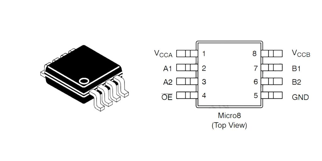
| Pin Number | Pin Name | Description |
|---|---|---|
| 1 | VCCA | Supply voltage for side A (0.9V~4.5V) |
| 2 | A1 | Channel 1 Input/Output (Side A) |
| 3 | A2 | Channel 2 Input/Output (Side A) |
| 4 | GND | Ground |
| 5 | OE | Output Enable (Active Low, pull-up for high-impedance state) |
| 6 | B2 | Channel 2 Input/Output (Side B) |
| 7 | B1 | Channel 1 Input/Output (Side B) |
| 8 | VCCB | Supply voltage for side B (0.9V~4.5V) |
When you’re wiring up the NLSV2T244DMR2G for voltage-level shifting, here’s what you need to keep in mind. First off, you’ve got two separate power pins—VCCA and VCCB—each supports voltages from 0.9V to 4.5V. The great part is, you don’t need a special startup order, but do add a small 0.1µF capacitor near each power pin for stable operation.
The signal pins, A1/A2 and B1/B2, are bidirectional, meaning you can choose which side sends or receives signals, based on your design. The OE pin is your output enable control—set it low to start data transfer, or high to put the outputs in a high-impedance state, ideal when sharing a bus with multiple devices.
Watch your input voltages carefully; never exceed the supply voltage on the corresponding side to avoid damaging the chip. Also, keep your PCB layout compact to reduce noise and interference, ensuring reliable, high-speed operation.
nlsv2t244dmr2g equivalent level translator

| Parameter/Model | NLSV2T244DMR2G (Original) | SN74LVC2T45DCTR (TI) | SN74AVC2T45DCTR (TI) | SN74LVC2T45DCUT (TI) |
|---|---|---|---|---|
| Package Type | Micro8 (MSOP-8) | SM8 (MSOP-8) | SM8 (MSOP-8) | VSSOP-8 |
| Channel Count | 2 | 2 | 2 | 2 |
| Supply Voltage Range | 0.9V – 4.5V | 1.65V – 5.5V | 1.2V – 3.6V | 1.65V – 5.5V |
| Data Rate | Unspecified | Up to 420 Mbps | Up to 380 Mbps | Up to 420 Mbps |
| Direction Control | Fixed Direction | Configurable (DIR Pin) | Configurable (DIR Pin) | Configurable (DIR Pin) |
| Tri-state Output Control | OE Pin Control | Supported | Supported | Supported |
| Typical Current Consumption | Low-power Design | 10 µA | 10 µA | 10 µA |
| Operating Temperature Range | -40°C to +85°C | -40°C to +85°C | -40°C to +85°C | -40°C to +85°C |
| ESD Protection Capability | HBM > 5000V | HBM > 4000V | HBM > 2000V | HBM > 4000V |
| Supports Short-circuit Protection | Yes | Yes | Yes | Yes |
| Supports Hot-swapping | Yes | Yes | Yes | Yes |
When you’re choosing a replacement chip, there are some key points you’ll want to keep in mind. First, double-check the voltage range—your new chip needs to match or exceed the original device’s operating voltage to ensure compatibility. Also, remember the original chip might have a fixed data direction, but replacements often have a configurable direction controlled by a DIR pin, so plan your logic accordingly.
Although the package might look identical, always verify each pin’s function carefully, since differences can cause unexpected issues. Speed matters too; make sure the new component supports your required data rates, ideally matching or outperforming your current chip.
Don’t forget ESD protection—if your project is in a noisy or industrial setting, choose a device with robust ESD ratings for better reliability. Finally, think practically about availability and cost; pick a readily available, cost-effective alternative to keep your project sustainable and economical. Always test thoroughly before finalizing the swap to ensure smooth operation.
nlsv2t244dmr2g level shifting circuit
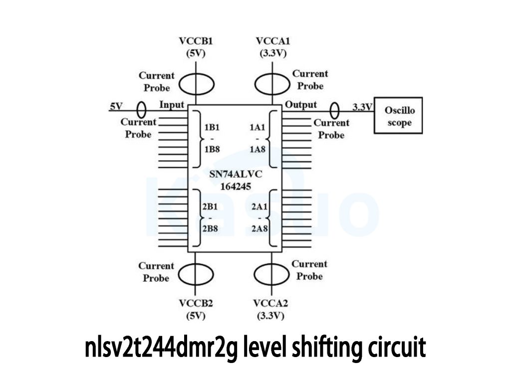
If you take a close look at this circuit diagram, you’ll see exactly how the NLSV2T244DMR2G chip handles level shifting between two different voltage domains. Notice how clearly labeled V_CCA and V_CCB are—that tells you right away this chip is designed for connecting signals between different logic voltages.
You’ve got two separate channels here (A1→B1 and A2→B2), which match perfectly with the chip’s dual-channel setup. There’s also the OE pin, your output-enable control: keep OE low to pass signals through, or set it high to put the outputs into a safe high-impedance state, preventing any bus conflicts.
Another nice thing you’ll notice is that the circuit uses two inverters in a row per channel, giving you a clean, non-inverted output, exactly like the NLSV2T244DMR2G’s intended behavior. Make sure your dual power rails (V_CCA and V_CCB) match your application voltages, and you’ll have smooth, reliable signal translation every time.
nlsv2t244dmr2g voltage translation example
When you’re connecting parts that run at different voltages, the NLSV2T244DMR2G chip is your go-to solution. It easily bridges low-voltage systems (like your 1.8V microcontrollers) and higher-voltage devices (like 3.3V sensors or displays), giving you reliable, clear signals without any inversion.
Inside, it has two separate channels—each handles one-way communication. When your input is high, the output stays high, and the same goes for low inputs. There’s an OE pin to control outputs; keep it low to let data flow, or high to safely disconnect outputs and avoid bus conflicts.
Another nice thing is you don’t need to worry about power-up sequences. Just connect each side’s voltage and add decoupling capacitors nearby. It’s also protected against accidental voltage spikes and power-down situations, keeping your hardware safe.
You’ll often use this chip in phones, FPGA interfaces, industrial controllers, or consumer electronics. Just remember: never feed an input higher than the supply voltage, and lay out your PCB carefully to maintain signal integrity.
nlsv2t244dmr2g bidirectional logic converter
Recommended Bidirectional Logic-Level Translator Models:
| Chip Model | Direction Control | Voltage Range | Data Rate | Manufacturer |
|---|---|---|---|---|
| TXB0102 | Automatic Bidirectional Detection | 1.2V ~ 3.6V | Up to 100 Mbps | TI |
| TXS0102 | Automatic Bidirectional Detection | 1.65V ~ 3.6V | Up to 24 Mbps | TI |
| SN74AVC2T45 | Manual Direction Control | 1.2V ~ 3.6V | Up to 500 Mbps | TI |
| NLSX3012 | Automatic Bidirectional Detection | 1.2V ~ 5.5V | Up to 100 Mbps | onsemi |
nlsv2t244dmr2g i2c spi voltage translation
1. Great for SPI Level Shifting
If you’re working with SPI communication—which has separate, single-directional data lines like MOSI and MISO—then the NLSV2T244DMR2G is a perfect choice. For example, maybe your MCU runs at 3.3V and your sensor at 1.8V; you can easily shift signals like MOSI, SCLK, or CS lines using this chip. Just keep in mind that MOSI and MISO need their own dedicated channels since they move data in opposite directions. But remember, if you’re dealing with single-wire bidirectional SPI, you’ll need a different solution because this chip only does one-way data flow.
2. Not Suitable for I²C Level Shifting (Important!)
However, you definitely shouldn’t use the NLSV2T244DMR2G for I²C interfaces. I²C requires signals to travel back and forth on the same line (both SDA and SCL), and this chip simply can’t do that. Instead, you’ll need specialized bidirectional translators like the NLSX3012 from onsemi, TI’s TXS0102, PCA9306, or the classic MOSFET-based level shifter using something like a BSS138 transistor.
More Like This

74HCT280D,653
NXP USA Inc.

74HCT280N,652
NXP USA Inc.
N74F280BN,602
NXP USA Inc.

1621B2UZZGR
Texas Instruments
1621B1UZZGR
Texas Instruments

SN74S280NSRG4
Texas Instruments

SN74LS280DRG4
Texas Instruments
SN74AS286NSRG4
Texas Instruments
SN74AS286DRG4
Texas Instruments
SN74AS280DRG4
Texas Instruments
SN74ALS280DRG4
Texas Instruments
SN74ALS280DG4
Texas Instruments
Also Add to Cart
AD812AR
Analog Devices Inc.

TDA7264
STMicroelectronics

XC7A50T-2CSG325C
AMD Xilinx
5AGXFB7H4F35I3G
Intel
.JPG "XC7A200T-1FBG676I")
XC7A200T-1FBG676I
AMD Xilinx

LCMXO2-640HC-4MG132I
Lattice Semiconductor Corporation

TLE42744G V50
Infineon Technologies

S912XEG384BCAA
NXP USA Inc.

TPS65132A0YFFR
Texas Instruments

DSPIC33EP256MC206T-I/PT
Microchip Technology

TPS3828-33DBVT
Texas Instruments

CY62256VNLL-70ZXI
Cypress Semiconductor Corp
Related Products
74HCT280D,653
NXP USA Inc.
74HCT280N,652
NXP USA Inc.
N74F280BN,602
NXP USA Inc.
1621B2UZZGR
Texas Instruments
1621B1UZZGR
Texas Instruments
SN74S280NSRG4
Texas Instruments
SN74LS280DRG4
Texas Instruments
SN74AS286NSRG4
Texas Instruments
SN74AS286DRG4
Texas Instruments
SN74AS280DRG4
Texas Instruments
SN74ALS280DRG4
Texas Instruments
SN74ALS280DG4
Texas Instruments

CY74FCT480BTSOCTG4
Texas Instruments
CD74AC280M96G4
Texas Instruments
74ACT11286NG4
Texas Instruments
74ACT11286N
Texas Instruments

SY10E193JZ TR
Microchip Technology
SY10E193JZ
Microchip Technology
SY10E160JZ TR
Microchip Technology
SY10E160JZ
Microchip Technology
SY100S360JZ-TR
Microchip Technology
SY100S360JZ
Microchip Technology
SY100E193JZ TR
Microchip Technology
SY100E193JZ
Microchip Technology
SY100E160JZ TR
Microchip Technology
SY100E160JZ
Microchip Technology
SN74S280NSRE4
Texas Instruments
SN74S280NSR
Texas Instruments
SN74LS280DRE4
Texas Instruments
SN74LS280DR
Texas Instruments
Please send RFQ , we will respond immediately.
