
MT29F2G08ABAEAH4:E datasheet, price, pdf
- Brands: Micron Technology Inc.
- Download: MT29F2G08ABAEAH4:E Datasheet PDF
- Price: inquiry
- In Stock: 15,477
- Memory Type: Non-Volatile
- Memory Format: FLASH
- Technology: FLASH - NAND
- Package: 63-VFBGA


FREE delivery for orders over HK$250.00

Quick response, quick quotaton

Flash shipment,no worries after sales

Original channel,guarantee of the authentic products
Mt29f2g08abaeah4:E
If you’re looking for reliable NAND flash storage, the MT29F2G08ABAEAH4:E from Micron is a great choice. This 2Gb (256MB) SLC NAND chip offers exceptional durability—perfect for frequent write and erase cycles. It runs smoothly between 2.7V and 3.6V, handles temperatures from -40°C to +85°C, and comes in a compact 63-ball VFBGA package. Its parallel interface meets ONFI 1.0 standards, ensuring compatibility with many controllers. Ideal for embedded systems, industrial control, consumer electronics, and data logging applications. Just be sure to check Micron’s datasheet for detailed integration guidelines or contact their authorized distributors for extra support.
Mt29f2g08abaeah4:E Pinout

| Pin Name | Type | Function Description |
|---|---|---|
| ALE | Input | Address latch enable; Latches input address on high level |
| CE# | Input | Chip enable signal; Active low |
| CLE | Input | Command latch enable; Latches command input on high level |
| RE# | Input | Read enable signal; Active low, used for reading data from chip |
| WE# | Input | Write enable signal; Active low, used for writing data into chip |
| WP# | Input | Write protection pin; Writing or erasing is disabled when low |
| R/B# | Output | Ready/Busy status pin; Low indicates busy, High indicates ready |
| I/O[7:0] | Bidirectional | Data input/output pins, used for transmitting commands, addresses, and data |
| VCC | Power | Power supply for the chip (2.7~3.6 V) |
| VSS | Power | Ground pin for the chip |
| NC | No Connection | Pin not connected internally; can be left floating or connected to ground |
| DNU | Reserved | Do Not Use pin; must be left floating |
When wiring up your MT29F2G08ABAEAH4:E NAND flash chip, keep a few things in mind. First, connect VCC to a steady 2.7–3.6V supply, and place a 0.1µF ceramic capacitor close by to keep power clean. Keep your ground line short to reduce noise. For signal pins like ALE, CLE, CE#, WE#, and RE#, route them short and match impedance to minimize interference. Pins like WP# and R/B# need pull-up resistors (10kΩ) to VCC. Never connect NC pins to signals or voltage, and always leave DNU pins floating to avoid damaging the chip. Lastly, always start with a RESET command (0xFF) after powering up.
Mt29f2g08abaeah4:E Equivalent Nand Flash
| Parameter | MT29F2G08ABAEAH4:E (Original) | MT29F2G08ABAGAH4-IT:G | K9F2G08U0C-SCB0 | TC58NVG2S0HTAI0 | W29N02GVSI |
|---|---|---|---|---|---|
| Manufacturer | Micron | Micron | Samsung | Toshiba | Winbond |
| Capacity | 2Gb (256MB) | 2Gb | 2Gb | 2Gb | 2Gb |
| Interface Type | Parallel NAND | Parallel NAND | Parallel NAND | Parallel NAND | Parallel NAND |
| Package Type | 63-ball VFBGA | 63-ball VFBGA | 63-ball VFBGA | 63-ball VFBGA | 63-ball VFBGA |
| Page Size | 2048+64 Bytes | 2048+64 Bytes | 2048+64 Bytes | 2048+64 Bytes | 2048+64 Bytes |
| Block Size | 128K+4K Bytes (64 pages) | 128K+4K Bytes | 128K+4K Bytes | 128K+4K Bytes | 128K+4K Bytes |
| Operating Voltage | 2.7–3.6 V | 2.7–3.6 V | 2.7–3.6 V | 2.7–3.6 V | 2.7–3.6 V |
| Operating Temperature | -40°C ~ +85°C | -40°C ~ +85°C | -40°C ~ +85°C | -40°C ~ +85°C | -40°C ~ +85°C |
| ONFI Compatibility | ONFI 1.0 | ONFI 1.0 | ONFI 1.0 | ONFI 1.0 | ONFI 1.0 |
| Endurance (P/E cycles) | 100,000 | 100,000 | 100,000 | 100,000 | 100,000 |
| Data Retention | 10 years | 10 years | 10 years | 10 years | 10 years |
If you’re swapping out your NAND flash chip for a different model, here’s what you need to watch out for. First, make sure the new chip’s package matches your original—otherwise, you’ll end up redesigning your PCB. Even with identical packages, double-check pin arrangements carefully; different brands might vary. Match the electrical specs like voltage ranges, page and block sizes to keep things compatible. It’s great if your chip supports the ONFI standard, but still verify that your controller can handle the replacement. Lastly, pick a chip rated for your specific temperature conditions. Always consult the manufacturer’s datasheets before making your final decision.
Mt29f2g08abaeah4:E Interface Circuit

When you’re wiring up your NAND flash chip, here’s the quick rundown. Connect the 8-bit data bus (I/O[7:0]) directly to your controller for data exchange. Then, you’ve got a few important control signals: CE# to activate the chip, RE# and WE# for reading and writing data, and ALE and CLE to latch address and command info. Don’t forget to pull WP# up to 3.3V through a 10k resistor—it stops accidental writes. Also, pull up R/B# similarly, so your controller can see if the chip’s busy or ready. Power-wise, connect VCC to a steady 3.3V supply and VSS straight to ground.
Mt29f2g08abaeah4:E Spi Nand Example
If you’re thinking about using the MT29F2G08ABAEAH4:E NAND flash chip, just remember it’s built for a parallel interface, which means it’ll communicate using multiple data lines (typically 8 bits) and dedicated control signals like CE#, WE#, RE#, ALE, and CLE. This design gives you high-speed data transfers and real-time performance, making it great for embedded systems, industrial controls, or data loggers.
But here’s the thing—it doesn’t support SPI, a simpler serial interface that transfers data one bit at a time using fewer pins (usually just four: CS, MOSI, MISO, and SCLK). SPI chips are perfect if your PCB space or GPIO pins are limited.
If your design requires SPI to simplify your layout or save resources, you’d be better off with dedicated SPI NAND chips, like MT29F1G01ABAFDWB or MT29F2G01ABAFDWB. These chips come with built-in SPI controllers, letting you easily achieve compact designs, cleaner wiring, and lower power usage.
Mt29f2g08abaeah4:E Timing Diagram

The timing diagrams for the MT29F2G08ABAEAH4:E NAND Flash include Reset, Read Status, Page Read, Page Program, and Block Erase operations. Below, I will focus specifically on the detailed timing description of the Read Status operation.
Let’s break down how the MT29F2G08ABAEAH4:E NAND flash performs a “Read Status” operation. First, you’ll send the status command (70h) to the chip. To do this, raise the CLE line high (this tells the chip you’re sending a command) and drop the CE# line low to select the device. Then, trigger a write by bringing the WE# line low—this latches the command into the chip through your data bus (I/O[7:0]).
After sending this command correctly (watch timing parameters like tCLS, tCS, and tWP carefully), you lower CLE to signal the end of the command phase. Now the chip is ready to respond.
Next, pull RE# low. This tells the chip to send its internal status onto the data lines. After a brief delay (tREA), the status appears on your data bus, ready for your controller to read. Once you’ve captured the status, bring RE# and CE# back high to finish up. The chip then returns to standby, waiting for your next command.
Mt29f2g08abaeah4:E Linux Driver
If you’re planning to use a NAND flash chip like the MT29F2G08ABAEAH4:E with Linux, it’ll usually run through the MTD (Memory Technology Device) subsystem, which makes working with raw flash memory easy. Linux divides NAND drivers into three main layers: the MTD layer for common commands (like read, write, erase), the NAND driver layer that manages specific NAND commands and timing, and the hardware controller layer, handling GPIO signals and data lines.
When you boot up, Linux first identifies your chip type by sending commands like Reset and Read ID, checking parameters such as page and block sizes. Then it handles your read/write requests by translating them into NAND-specific commands (like 00h for reads or 80h and 10h for page programming). The driver also manages ECC to keep your data error-free and tracks bad blocks, so your system stays reliable long-term.
Mt29f2g08abaeah4:E Boot Memory Usage
If you’re designing an embedded system and plan to use the MT29F2G08ABAEAH4:E NAND Flash as your boot memory, here’s how it works. At startup, your processor’s internal ROM communicates with the NAND through a dedicated controller. It grabs the bootloader (like U-Boot) stored on the NAND, loads it into RAM, and then executes it.
But here’s something important: NAND Flash can sometimes have bad blocks or bit errors. To deal with this, you’ll want to make sure your boot process includes error correction (ECC) and proper bad-block management. This helps ensure your system boots reliably every single time.
Typically, you’d partition the NAND chip to store the bootloader, operating system kernel, and your root filesystem separately. Doing this creates an organized structure, making sure your system starts smoothly and your data stays safe.
Mt29f2g08abaeah4:E Page/Block Architecture
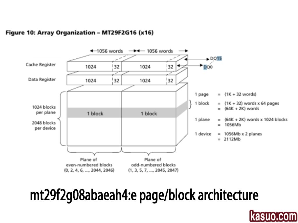
If you’re working with an MT29F2G16 NAND Flash chip, let me break down its storage structure for you in simple terms. Each memory page is made of 1056 words: 1024 words for your actual data and an extra 32 words called OOB space, used for things like error correction (ECC) and managing bad blocks.
These pages are grouped into blocks—each block contains 64 pages, totaling 66K words (64K for data plus 2K for OOB). On top of that, blocks are organized into larger sections called planes, with each plane having 1024 blocks, giving you about 1056Mb of storage per plane.
Your entire chip has two planes (one handling odd-numbered blocks, the other even-numbered ones), adding up to 2048 blocks and a full capacity of 2112Mb, or about 2Gb in total. Understanding this layout helps you manage data more effectively and keeps your system organized.
More Like This

CBTL06GP213EE
NXP Semiconductors

MAX458EPL
Analog Devices / Maxim Integrated
ADG5412FBCPZ
Analog Devices
ADG5412BFBCPZ
Analog Devices
ADG854BCPZ
Analog Devices
DG187AA
Vishay / Siliconix

74LVC1G66GV
Nexperia
FSA2275A
onsemi
TC4066BP
Toshiba
74LVC2G66DP
Nexperia
74LVC1G66GW
Nexperia
ADG1414BCPZ
Analog Devices
Also Add to Cart

SN74AHC16244DL
Texas Instruments

C8051F022
Silicon Labs

SP3232EEN
UMW
NJM2068M-TE1
Nisshinbo Micro Devices Inc.

NCP451FCT2G
onsemi

OB2361MP
OB(On-Bright Elec)

ATTINY26-16SUR
Microchip Technology

XC2S400E-6FT256I
AMD / Xilinx

ISL3178EIBZ-T
Renesas Electronics America Inc

LMR23630ADDA
Texas Instruments

10M04DAU324C8G
Intel
ATMXT2952T2-C2UR057
Microchip Technology
Related Products
CBTL06GP213EE
NXP Semiconductors
MAX458EPL
Analog Devices / Maxim Integrated
ADG5412FBCPZ
Analog Devices
ADG5412BFBCPZ
Analog Devices
ADG854BCPZ
Analog Devices
DG187AA
Vishay / Siliconix
74LVC1G66GV
Nexperia
FSA2275A
onsemi
TC4066BP
Toshiba
74LVC2G66DP
Nexperia
74LVC1G66GW
Nexperia
ADG1414BCPZ
Analog Devices

MAX4649EKA
Analog Devices / Maxim Integrated
74HC1G66GW
Nexperia
74LVC4066PW
Nexperia
ADG702BRTZ
Analog Devices
ADG701BRTZ
Analog Devices

ADG1219BRJZ
Analog Devices

74HCT4066D
Nexperia
ADG819BRTZ
Analog Devices
HEF4066BT
Nexperia

74HC4066PW
Nexperia
ADG1436YCPZ
Analog Devices
74HC1G66GV
Nexperia
ADG802BRTZ
Analog Devices
CLC018AJVJQ
Texas Instruments
HEF4014BT
Nexperia

74HCT165D
Nexperia

MC14094BCP
onsemi
74HCT164D
Nexperia
Please send RFQ , we will respond immediately.
