
MAX2771ETI+ datasheet, price, pdf
- Brands: Analog Devices Inc./Maxim Integrated
- Download: MAX2771ETI+ Datasheet PDF
- Price: inquiry
- In Stock: 206
- Modulationor Protocol: BeiDou, Galileo, GLONASS, GNSS, GPS
- Applications: General Purpose
- Data Interface: SPI
- Package: 28-WFQFN Exposed Pad


FREE delivery for orders over HK$250.00

Quick response, quick quotaton

Flash shipment,no worries after sales

Original channel,guarantee of the authentic products
MAX2771ETI+ Pinout Equivalent Circuit
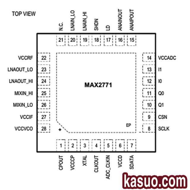
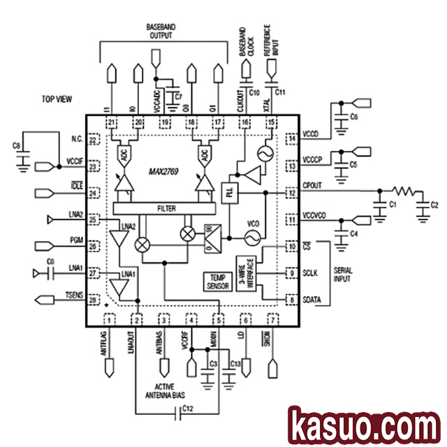
MAX2771ETI+ is a multi band universal GNSS receiver launched by Analog Devices.This chip supports global navigation satellite systems such as GPS,Galileo,GLONASS,BeiDou,IRNSS, QZSS, and SBAS,and can cover multiple frequency bands such as E1/L1,L2,L5, E5,E6,B1,B2,B3, etc. The chip integrates a complete receiving link internally, including a dual input low-noise amplifier(LNA), mixer, internal single-chip filter, programmable gain amplifier(PGA),multi bit analog-to-digital converter(ADC), and crystal oscillator circuit.Its total cascaded noise figure can reach a minimum of 1.4dB,and it can provide a cascaded gain of up to 110 dB and a gain control range of 59dB.Due to the high integration level of the chip,only a small number of peripheral components are needed.
MAX2771ETI+adopts QFN-28-EP (5×5), and its pin functions can be roughly divided into RF front-end, digital interface, PLL and clock, power supply and control modules. The following table lists some of the main pins and their functional descriptions:
| Pin | Name | Function |
|---|---|---|
| 1 | CPOUT | The output of the charge pump is connected to the PLL loop filter |
| 2 | VCCCP | Provide power to PLL |
| 3 | XTAL | Input pins of crystal oscillator |
| 4 | CLKOUT | Reference clock output pin |
| 5 | ADC_CLKIN | ADC clock input, optional, this pin provides external clock for ADC |
| 6 | VCCD | Provide power for digital circuits |
| 7 | SDATA | Three wire serial interface data signal |
| 8 | SCLK | The clock input of the three wire serial interface uses data for the rising edge and outputs data for the falling edge |
| 9 | CSN | Three wire serial chip selection input, low level effective |
| 10 | Q1 | Q-channel voltage output |
| 11 | Q0 | Q-channel voltage output |
| 12 | I0 | Channel I voltage output |
| 13 | I1 | Channel I voltage output |
| 14 | VCCADC | ADC power supply voltage |
| 15 | ANAIPOUT | Simulate I+channel output, directly suspended without use |
| 16 | ANAINOUT | Simulate I-channel output, directly suspended without use |
| 17 | LD | Phase lock detector output, high level represents PLL lock |
| 18 | SHDN | Chip control pin, low level can turn off the entire chip |
| 19 | LNAIN_HI | High frequency LNA input port requires external matching circuit |
| 20 | LNAIN_LO | Low frequency LNA input port, requires external matching circuit |
| 21 | NC | Connectionless |
| 22 | VVCCRF | Power supply voltage of RF module |
| 23 | LNAOUT_LO | Low frequency LNA output |
| 24 | LNAOUT_HI | High frequency LNA output |
| 25 | MIXIN_HI | High frequency mixer input |
| 26 | MIXIN_LO | Low frequency mixer input |
| 27 | VCCIF | Provide power to the IF module |
| 28 | VCCVCO | VCO power supply voltage |
Alternative model selection:
Due to the high integration and strong performance of MAX2771ETI+in the field of multi frequency GNSS reception, there are almost no substitute models that can fully match it. However, if only partial similarity in functionality and interface is required, and partial substitution of lower level products is needed, the following are several products that are similar to MAX2771ETI+in certain key parameters:
| Picture | Name | Constellation Support | Noise Figure | Package |
|---|---|---|---|---|
 |
MAX2769C | GPS/GLONASS/Galileo/Beidou System | 1.4 dB | QFN-28-EP (5×5) |
 |
MAX2769 | GPS/GLONASS/Galileo | 1.4 dB | QFN-28-EP (5×5) |
 |
MAX2769B | GPS/GLONASS/Galileo/Beidou System | 1.4 dB | QFN-28-EP (5×5) |
Application circuit and precautions:
In most cases, the GNSS front-end circuit design with MAX2771ETI+as the core requires external antennas to introduce satellite signals into the high-frequency and low-frequency LNA input terminals through a 50 Ω matching network to ensure maximum signal energy transmission and reduce losses caused by reflection. The power supply usually uses a single power supply (2.7-3.3V), and low ESR ceramic capacitors (usually 100nf) are placed near key pins such as VCCCP, VCCRF, VCCADC, VCCVCO, and VCCD to stabilize power supply and suppress power noise. The external crystal oscillator provides a high-precision, low phase noise reference clock through the XTAL pin, which supplies clock signals to the internal PLL and frequency divider. The chip can communicate data with microcontrollers or FPGA devices through SPI interfaces (CSN, SDATA, SCLK), making it easy to configure registers and collect data. The overall PCB design requires the RF signal path to be as short as possible, the routing impedance to be executed according to requirements, and the analog and digital parts to be completely separated. At the same time, the exposed solder pads should be closely integrated with the large-area ground plane to improve heat dissipation and shielding effects.
More Like This

2095100001200
HARTING
20953000002
HARTING
2095100000101
HARTING
20953000060
HARTING
2095100001600
HARTING
20953000082
HARTING
20953000013
HARTING
2095100000500
HARTING
20953000036
HARTING
20953000054
HARTING
2095100000800
HARTING
20953000600
HARTING
Also Add to Cart

BIS0102
Balluff

HMC1121LP6GE
Analog Devices Inc.

BMD-301-A-R
u-blox
.JPG "PD4859J5050S2HF")
PD4859J5050S2HF
TTM Technologies, Inc.
DAT-31R5A-PP+
Mini-Circuits
HMC580ST89E
Analog Devices Inc.

WT41U-E-AI56
Silicon Labs

ANFCA-6040-A02
Abracon LLC

HMC129ALC4
Analog Devices Inc.

SKY13317-373LF
Skyworks Solutions Inc.

HMC432
Analog Devices Inc.

SKY13374-397LF
Skyworks Solutions Inc.
Related Products
2095100001200
HARTING
20953000002
HARTING
2095100000101
HARTING
20953000060
HARTING
2095100001600
HARTING
20953000082
HARTING
20953000013
HARTING
2095100000500
HARTING
20953000036
HARTING
20953000054
HARTING
2095100000800
HARTING
20953000600
HARTING
20953000091
HARTING
20953000079
HARTING
2095100001800
HARTING
20953000027
HARTING
20953000011
HARTING
20953000047
HARTING
20953000004
HARTING
2095100002200
HARTING
20953000076
HARTING
2095100001100
HARTING
20953000044
HARTING
20953000003
HARTING
20953000008
HARTING
20953000086
HARTING
20953000012
HARTING
2095100002500
HARTING
2095100001700
HARTING
2095300007100
HARTING
Please send RFQ , we will respond immediately.
