
LNK564PN pinout | circuit diagram | datasheet
- Output Isolation: Isolated
- Topology: Flyback
- Fault Protection: Current Limiting, Open Loop, Over Temperature, Short Circuit
- Package: 8-PDIP-B


FREE delivery for orders over HK$250.00

Quick response, quick quotaton

Flash shipment,no worries after sales

Original channel,guarantee of the authentic products
{276} LNK564PN, Datasheet, Application Circuit Diagram, Equivalent, for LNK562, LNK563 & LNK564 Urdu
LNK564PN Pinout
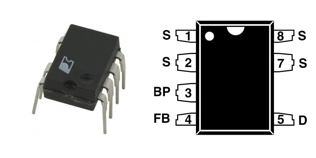
| Pin Number | Pin Name | Description |
|---|---|---|
| 1 | S | Source – High-voltage power MOSFET source connection. |
| 2 | S | Source – Internally connected to pin 1, provides heat sinking and return path. |
| 3 | BP | Bypass – Connect a capacitor to this pin to provide internal supply filtering. |
| 4 | FB | Feedback – Receives feedback signal from the output to regulate switching. |
| 5 | D | Drain – High-voltage input and power MOSFET drain terminal. |
| 7 | S | Source – Same function as pins 1 and 2. |
| 8 | S | Source – Same as above, provides additional thermal and electrical path. |
The LNK564PN is a highly integrated offline switcher IC used in low-power AC-DC converters. When using the pinout:
Pin 3 (BP) must be connected to a bypass capacitor (typically 0.1 μF) to stabilize the internal supply.
Pin 4 (FB) is used for feedback regulation and should be connected through an optocoupler or resistor network to maintain output voltage regulation.
Pin 5 (D) connects directly to the high-voltage DC bus (after rectification).
Pins 1, 2, 7, and 8 (S) are internally tied together and must be connected to ground (or source) with a low-impedance path, ensuring good thermal and electrical performance.
Important:
Do not use or connect a non-existent Pin 6; it is intentionally omitted in the package design. Ensure adequate PCB layout for thermal dissipation, especially around the source pins.
LNK564PN Circuit Diagram
LNK564PN is an integrated IC commonly used in low-power flyback switching power supply designs, with low cost, low power consumption, high efficiency, and few external components. In this article, we will introduce the principle and structure of low-power integrated switching power supply ICs LNK564PN
1、LNK564PN Principle
LNK564PN is a controller switch IC that provides up to 3 W of output power due to its cost-effective alternative to power supplies based on unregulated isolated linear transformers (50/60 Hz). It is a design based on a single common input instead of multiple linear transformers. The self-made bias circuit outputs very low no-load power consumption of 150 mW. Internal oscillator frequency jitter to the symbol Fi does not reduce the quasi-peak sum
Average EMI, optimize filter cost
2. LNK564PN Internal structure circuitry
The internal structure of the chip consists of a 700 V power MOSFET switch and a power controller. Unlike traditional PWM (Pulse Width Modulation) controllers, it uses simple ON/OFF control to regulate the output voltage. The controller consists of an oscillator, feedback (sensing and logic) circuitry, a 5.8 V regulator, BP pin undervoltage circuitry, overtemperature protection, frequency jitter, current limiting circuitry, and leading-edge blanking. The compact structure facilitates PCB layout and routing, as shown in the figure LNK564PN Functional Block Diagram
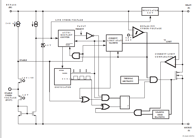
LNK564PN Internal Circuit Diagram
3. Classical circuit analysis
Input stage: BR1 rectifier bridge + C/L filtering
Transformer: E-type core, the ratio of turns of secondary to bias winding determines the output voltage of 25V.
Output stage: secondary rectifier diode (e.g., 1N4007) + filter capacitor (e.g., 470μF) 24V.
Feedback network: Resistor divider (R1/R2) or Zener diode (VR) connected to FB pin
LNK564PN the advantages of high efficiency, low cost, small number of components, high parameter accuracy, and use proprietary IC fine-tuning technology and transformer structure technology; Precise parameter tolerances enable clamping design, reduce costs and improve efficiency; Meets the industry standard requirements for thermal overload protection, hysteresis thermal shutdown protection and auto-recovery to prevent overheating damage improves field reliability, low-cost input filtering configuration, and the IC enters auto-restart mode when the output is short-circuited or open-loop, limiting the output power to ≥85% of normal.

LNK564DN Classic circuitry
More Like This

CBTL06GP213EE
NXP Semiconductors

MAX458EPL
Analog Devices / Maxim Integrated
ADG5412FBCPZ
Analog Devices
ADG5412BFBCPZ
Analog Devices
ADG854BCPZ
Analog Devices
DG187AA
Vishay / Siliconix

74LVC1G66GV
Nexperia
FSA2275A
onsemi
TC4066BP
Toshiba
74LVC2G66DP
Nexperia
74LVC1G66GW
Nexperia
ADG1414BCPZ
Analog Devices
Also Add to Cart

EP1C12Q240I7
Intel

AD202JY
Analog Devices Inc.

74ACT125SCX
onsemi

DSPIC33FJ128MC804-I/PT
Microchip Technology

CY8CMBR3108-LQXI
Cypress Semiconductor Corp
BCM53286MIPBG
Broadcom Limited

TMS320F28069MPZT
Texas Instruments

ATT7039AU
HiTrend Tech (Shanghai)

LM2575SX-5.0
Texas Instruments

TS12A12511DCNR
Texas Instruments

RM48L952DPGET
Texas Instruments

M25P128-VMF6PB
Micron
Related Products
CBTL06GP213EE
NXP Semiconductors
MAX458EPL
Analog Devices / Maxim Integrated
ADG5412FBCPZ
Analog Devices
ADG5412BFBCPZ
Analog Devices
ADG854BCPZ
Analog Devices
DG187AA
Vishay / Siliconix
74LVC1G66GV
Nexperia
FSA2275A
onsemi
TC4066BP
Toshiba
74LVC2G66DP
Nexperia
74LVC1G66GW
Nexperia
ADG1414BCPZ
Analog Devices

MAX4649EKA
Analog Devices / Maxim Integrated
74HC1G66GW
Nexperia
74LVC4066PW
Nexperia
ADG702BRTZ
Analog Devices
ADG701BRTZ
Analog Devices

ADG1219BRJZ
Analog Devices

74HCT4066D
Nexperia
ADG819BRTZ
Analog Devices
HEF4066BT
Nexperia

74HC4066PW
Nexperia
ADG1436YCPZ
Analog Devices
74HC1G66GV
Nexperia
ADG802BRTZ
Analog Devices
CLC018AJVJQ
Texas Instruments
HEF4014BT
Nexperia

74HCT165D
Nexperia

MC14094BCP
onsemi
74HCT164D
Nexperia
Please send RFQ , we will respond immediately.
