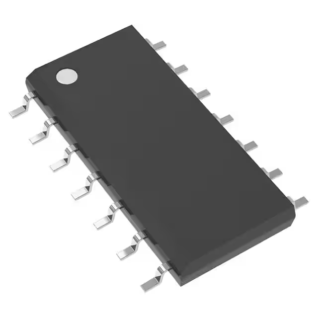
LMC555CN pinout | circuit | timer datasheet Texas Instruments
- Type: 555 Type, Timer/Oscillator (Single)
- Frequency: 3MHz
- Voltage-Supply: 1.5V ~ 15V
- Package: 8-DIP (0.300, 7.62mm)
LMC555CN Pinout Equivalent

1:Overview of the LMC555CN:
The LMC555CN is a timer chip based on CMOS technology. Compared to traditional 555 timers, the LMC555CN uses CMOS processes, significantly reducing power consumption, making it excellent for battery-powered devices with high power requirements. The LMC555CN operates over a wide voltage range of 2V to 18V and typically functions within a temperature range of -40°C to 85°C, ensuring stable performance in harsh environments. Its astable mode can generate pulse signals of different frequencies and duty cycles, suitable for clock signals and modulation signals in electronic devices.
2:LMC555CN Important pin function definition:
| Pin Number | Pin Name | Description |
|---|---|---|
| Pin1 | GND | Ground terminal provides circuit reference ground. |
| Pin2 | TRIG | Low-level triggered input terminal. – When the voltage < 1/3 Vcc, trigger the monostable mode or flip the output. |
| Pin3 | OUT | Output terminal, which can output high/low level. – High level is close to Vcc, and low level is close to GND. – Maximum drive current < 50mA (CMOS characteristic). |
| Pin4 | RESET | Reset terminal. – When connected to low level (≤0.4V), it forces the output to low level and disables the timer function. |
| Pin5 | CTRL | Control voltage input terminal. – By default, it is grounded through a 0.01 µF capacitor. The threshold and trigger levels can be adjusted. – When a voltage is directly input, the threshold level is CTRL voltage, and the trigger level is 1/2 CTRL voltage. |
| Pin6 | THR | High-level threshold input terminal. – When the voltage is > 2/3 Vcc (by default) or > CTRL voltage, a low-level output is triggered. |
| Pin7 | DISCH | Discharge terminal, connected to the drain of the internal CMOS transistor. – When outputting high level, floating (high impedance state). When outputting low level, grounded. |
| Pin8 | VCC | Power input terminal, voltage range 1.5V – 15V (supports battery power supply). |
3:Alternative model recommendation
TLC555IDR: Adopting CMOS technology, it has low power consumption. The power supply voltage range is 2V – 18V. It has high input impedance, and the output can directly drive CMOS circuits.

MC1455BDR2G: Also based on CMOS technology, with low power consumption. The operating voltage range is 3V – 15V. It has three working modes (monostable, astable, and bistable) similar to LMC555CN.

NE555DR: Classic bipolar timer chip with wide applications. The power supply voltage range is 4.5V – 16V, and it has strong output driving ability.

MAX7219: Strictly speaking, it is not a traditional replacement for the 555 timer. However, it can be an option in some timing and display control applications. It is an integrated display driver that can be used to drive multiple seven-segment digital tubes and has certain timing and control functions.

More Like This
Also Add to Cart
MPQ3367GR-AEC1-Z
Monolithic Power Systems Inc.
PT4115
UMW
PT4115
EVVO
TPS92665QPHPRQ1
Texas Instruments
LT8355IUFDM-1#WPBF
Analog Devices Inc.
MP4056GS-Z
Monolithic Power Systems Inc.
TPS929240QDCPRQ1
Texas Instruments
HMC765LP6CE
Analog Devices Inc.
SI5347A-B-GM
Skyworks Solutions Inc.
HMC807LP6CE
Analog Devices Inc.


