INA219AID datasheet | connection & current sensor
- Function: Current Monitor
- Sensing Method: High-Side
- Accuracy: ±1%
- Package: 8-SOIC (0.154, 3.90mm Width)


FREE delivery for orders over HK$250.00

Quick response, quick quotaton

Flash shipment,no worries after sales

Original channel,guarantee of the authentic products
INA219 Pinout

INA219 Pinout Picture
INA219 is a zero-drift bi-directional current monitoring chip with IIC interface (zero-drift: roughly means that it is very accurate, there will be no current drift); the monitoring port can withstand a voltage of 0 to 26V is a very wide range of operating voltages; with 16 programmable addresses, you can read or control the chip through the IIC; high precision, in the appropriate operating temperature range of the accuracy of the accurate to 0.5%; the package is SOT23-8 or SOIC-8 two package form; mainly used in, rechargeable batteries, chargers and other devices. High precision, within the appropriate operating temperature range, the accuracy can be accurate to 0.5%; the package is SOT23-8 or SOIC-8 two package forms; mainly used in, rechargeable treasure, chargers and other equipment.
The specific pin definitions are as follows:
| Pin | Symbol | Description |
|---|---|---|
| 1 | IN+ | Inflow port for current detection |
| 2 | IN- | Outflow port for detecting current |
| 3 | GND | Used as a ground in circuit diagram design |
| 4 | VS | As the positive terminal of the power supply |
| 5 | SCL | Clock port for IIC communication |
| 6 | SDA | Port for transmitting data for IIC communication |
| 7 | A0 | Slave address selection pin |
| 8 | A1 | The slave’s address selection pin is used in conjunction with A0 |
INA219 Circuit

ina219 Picture
The INA219 is a commonly used high-precision current, voltage and power detection chip from Texas Instruments. It is widely used in battery charging and discharging circuits, mobile phone chargers, solar chargers and various electronic circuits that require accurate detection of current, voltage and power parameters. INA219 can communicate with the microcontroller through the IIC communication protocol, and we can use the microcontroller to send instructions to INA219 to obtain various information collected by it. Next, we will introduce the detailed parameters of INA219 and the reference design of the circuit.
Basic parameters of INA219:
Bus voltage range: 0~26V ‘
Current measurement range: according to the peripheral resistance configuration to determine (maximum support 3.2A);
Power measurement range: calculated from the measured value of voltage and current;
Measurement accuracy: the maximum error is 0.5%;
INA219 circuit diagram design;
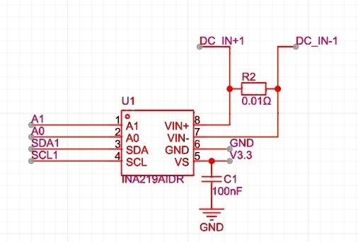
INA219 circuit diagram
As shown in the figure, the chip requires very few peripheral circuits to work; First look at pins 1 and 2 are the address of the device; The microcontroller uses this address (00,01,10,11) to identify which slave device it is. The 3、4 pins are SDA and SCL pins respectively used to communicate with the MCU. Theoretically, a 4.7K pull-up resistor is required here, but considering that most MCU GPIO has its own pull-up resistor; The other pins are clearly visible from the circuit; 7、8 is the input pin of the device to be tested, 6 is GND, and 5 is the chip power supply port, which is connected after a capacitor filter. R2 is used to collect the resistance, the official manual is used in 0.01 ohms, in actual use can be selected according to the need to collect the range of parameters.
More Like This

GAL22V10D-10LD/883
Lattice

EPM7192SQI160-10N
Altera
AD2410WCCSZ-RL
Analog Devices
AD2425WCCSZ
Analog Devices
XCZU15EG
AMD / Xilinx
XAZU2EG
AMD / Xilinx
XC7Z010
AMD / Xilinx
10AS016E3F29E2SGHZ
Altera
HCPL-7860-50YE
Broadcom / Avago

AD2S83AP
Analog Devices
AD7147PACPZ
Analog Devices
AD7147ACPZ
Analog Devices
Also Add to Cart

AD7680BRMZ
Analog Devices Inc.

L7805ACD2T-TR
STMicroelectronics

MPQ4423AGQ-AEC1-Z
Monolithic Power Systems Inc.
.jpg "NCP43080DMTTWG")
NCP43080DMTTWG
onsemi

PIC12LF1822-I/MF
Microchip Technology

ADR445BRZ-REEL7
Analog Devices Inc.

NJM2360AM
Nisshinbo Micro Devices Inc.

ST2378ETTR
STMicroelectronics

AT89C2051-24SU
Microchip Technology

SC33771CTA1MAE
NXP USA Inc.

LP38693SD-ADJ
Texas Instruments

S25FL032P0XMFI011
Cypress Semiconductor Corp
GAL22V10D-10LD/883
Lattice
EPM7192SQI160-10N
Altera
AD2410WCCSZ-RL
Analog Devices
AD2425WCCSZ
Analog Devices
XCZU15EG
AMD / Xilinx
XAZU2EG
AMD / Xilinx
XC7Z010
AMD / Xilinx
10AS016E3F29E2SGHZ
Altera
HCPL-7860-50YE
Broadcom / Avago
AD2S83AP
Analog Devices