
EPCQ64SI16N datasheet & marking | component details
- Product Status: Obsolete
- Programmable Type: In System Programmable
- Memory Size: 64Mb
- Package: 16-SOIC (0.295, 7.50mm Width)


FREE delivery for orders over HK$250.00

Quick response, quick quotaton

Flash shipment,no worries after sales

Original channel,guarantee of the authentic products
Epcq64si16n
The EPCQ64SI16N chip is a handy Quad-SPI NOR Flash memory designed specifically for storing your configuration data. It gives you 64 Mbit (that’s about 8 MB) of storage space, ideal for various applications. It supports both standard SPI and Quad SPI interfaces, delivering data transfer speeds up to 50 MHz—great for fast performance.
This chip operates reliably at voltages between 2.7 V and 3.6 V and comes packaged neatly in a 16-pin SOIC, just 7.5 mm wide. It’s built tough enough for industrial environments, handling temperatures from -40°C up to 85°C. Plus, it’s incredibly durable—good for up to 100,000 program/erase cycles and capable of retaining your data for about 20 years at 85°C.
For added security, it features block protection to prevent accidental erasure. Best of all, you can program it directly in your system without having to remove the chip, making updates super convenient.
Epcq64si16n Pinout

| Pin Number | Pin Name | Type | Function Description |
|---|---|---|---|
| 1 | CS# | Input | Chip Select (Active Low) |
| 2 | DQ0 | I/O | Data Line 0 (MOSI) |
| 3 | DQ1 | I/O | Data Line 1 (MISO) |
| 4 | DQ2 | I/O | Data Line 2 (WP#, Write Protect) |
| 5 | DQ3 | I/O | Data Line 3 (HOLD#, Pause) |
| 6 | VCC | Power | Positive Power Input (2.7V to 3.6V) |
| 7 | GND | Power | Ground (0V) |
| 8 | CLK | Input | Clock Input (Up to 50 MHz) |
| 9–16 | NC | — | Reserved, Do not connect or handle per design requirements |
When you’re setting up the EPCQ64SI16N, make sure you choose between the standard SPI or Quad SPI interface depending on your project needs. Pay careful attention to your power connections—your VCC should be between 2.7V and 3.6V, and your ground (GND) should be solidly connected.
If you’ve got any unused pins, like the NC pins, it’s best to either leave them floating or connect them to ground to minimize interference. For the CLK pin, supply it with a stable clock signal up to 50 MHz to keep your data transfers smooth and reliable.
The WP# (DQ2) and HOLD# (DQ3) pins are there to help you protect your data or pause your transfers, so double-check these signals are set correctly according to your specific application. Lastly, the chip comes in a compact 16-pin SOIC package that’s just 7.5 mm wide, perfect for most standard PCB designs.
Epcq64si16n Equivalent


| Parameter | EPCQ64SI16N | EPCQ64ASI16N | EPCQ128SI16N | EPCQ256SI16N | EPCQ512ASI16N |
|---|---|---|---|---|---|
| Manufacturer | Intel (Altera) | Intel (Altera) | Intel (Altera) | Intel (Altera) | Intel (Altera) |
| Memory Capacity | 64 Mbit | 64 Mbit | 128 Mbit | 256 Mbit | 512 Mbit |
| Interface Type | SPI/QSPI | SPI/QSPI | SPI/QSPI | SPI/QSPI | SPI/QSPI |
| Package Type | 16-pin SOIC | 16-pin SOIC | 16-pin SOIC | 16-pin SOIC | 16-pin SOIC |
| Operating Voltage | 2.7~3.6 V | 2.7~3.6 V | 2.7~3.6 V | 2.7~3.6 V | 2.7~3.6 V |
| Operating Temperature | -40°C ~ +85°C | -40°C ~ +85°C | -40°C ~ +85°C | -40°C ~ +85°C | -40°C ~ +85°C |
| Availability Status | Discontinued | In Stock | In Stock | In Stock | In Stock |
When choosing your memory chip, remember all these options come in the same 16-pin SOIC package—same size and pin layout. That means you can swap them out easily without changing your PCB design.
If your current 64Mbit capacity does the job, then the EPCQ64ASI16N is your simplest choice. But if you anticipate needing more space in the future, you might want to consider stepping up to a larger memory size like 128Mbit or 256Mbit.
Don’t worry about compatibility—all these chips use the same interfaces and operate within identical voltage ranges. So, you won’t have to tweak any of your existing circuitry.
Also, pick a chip that’s readily available, like the EPCQ64ASI16N or a larger version. That way, you avoid supply issues and ensure your project stays smooth and reliable in the long run.
Epcq64si16n Spi Interface Circuit
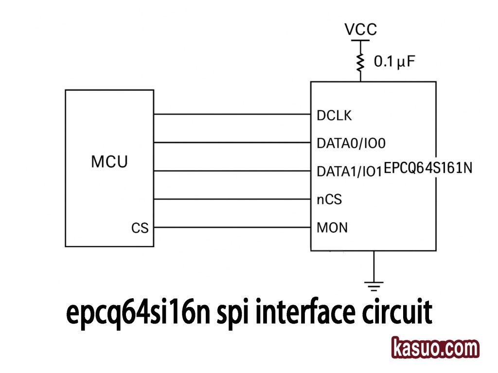
Your MCU should provide the SPI clock (DCLK) directly to the EPCQ64SI16N. Connect DATA0 (IO0/MISO) and DATA1 (IO1/MOSI) properly to the MCU’s MISO and MOSI pins, respectively. Make sure the nCS (chip select) line is clearly managed by your MCU. Good job on clearly connecting the chip’s power and ground, and it’s great you included a 0.1μF bypass capacitor to reduce noise.
However, watch out for the MON pin; unless you’ve got a specific use case, it’s usually best to leave it unconnected. Also, consider adding a larger capacitor, like a 1μF to 10μF electrolytic capacitor, parallel to your existing 0.1μF capacitor for even better power stability. When routing your SPI lines on the PCB, keep them short to reduce interference. If you’re dealing with high-speed SPI communication, it’s helpful to place small resistors (around 22Ω to 47Ω) in series with your SPI signals to improve signal quality and impedance matching.
Epcq64si16n Altera Configuration Memory
When you’re working with FPGA or CPLD systems, you’ll find this memory chip perfect for storing configuration files. It lets your FPGA automatically load the necessary settings as soon as it powers up, simplifying your design process.
If you’re building embedded systems around FPGAs, you can rely on this chip to store your boot code, firmware, and user programs securely. For communication equipment like routers or base stations, it safely holds FPGA configurations and essential parameters.
It’s also ideal for industrial control systems, giving you a stable storage solution for programmable logic arrays that handle critical control tasks and interface drivers. In data acquisition and measurement setups, it ensures your FPGA’s logic and signal processing run smoothly.
For video and image processing applications, it stores FPGA settings to enable efficient real-time performance. And if you’re designing automotive electronics or traffic control systems, this chip ensures your FPGA logic configurations stay highly reliable and ready for demanding environments.
Epcq64si16n Programming With Quartus
First, connect your EPCQ64SI16N chip’s SPI pins—nCS, DCLK, DATA0, DATA1, VCC, and GND—to your FPGA’s AS interface or your USB-Blaster programming interface.
Next, launch Quartus Prime software on your computer. Go to the Tools menu and select Programmer. In the Programmer window, set the mode to Active Serial Programming. You can either click Auto Detect to automatically recognize your chip or select EPCQ64 manually.
Once your chip is recognized, hit Add File to load the configuration file (.jic file) you’ve prepared earlier. Make sure to check the Program/Configure box, then click Start to begin programming.
It’ll take just a few moments—Quartus Prime will confirm when programming finishes successfully. After this, every time your FPGA powers up, it’ll automatically load the configuration from the EPCQ64SI16N, initializing the chip smoothly and efficiently.
Epcq64si16n Jtag Connection
| EPCQ64SI16N (SPI Interface) | FPGA (AS/JTAG Interface) | USB-Blaster Download Interface |
|---|---|---|
| nCS | nCS (AS_nCS) | TMS |
| DCLK | DCLK (AS_CLK) | TCK |
| DATA0 (IO0) | DATAOUT (AS_DO) | TDO |
| DATA1 (IO1) | DATAIN (AS_DATA) | TDI |
| VCC | 3.3V | 3.3V |
| GND | GND | GND |
When you’re working with the EPCQ64SI16N, keep in mind it usually doesn’t connect directly to JTAG. Instead, you’ll connect it through your FPGA’s Active Serial (AS) interface. From there, you’ll use the FPGA’s JTAG connection to program it indirectly.
In Quartus, make sure you’re selecting the Active Serial (AS) programming mode, which lets you program the chip indirectly through the JTAG chain.
Also, double-check that your power supply is stable at 3.3V and your grounding is solid. Keep your SPI signal wires as short as possible—this reduces interference and ensures your signals stay clean and reliable.
Epcq64si16n Fpga Bitstream Storage
If you’re working with an FPGA system, the EPCQ64SI16N chip is perfect for storing your FPGA’s configuration bitstream. Basically, when your FPGA powers up, it needs to load this bitstream file to initialize properly. The EPCQ64SI16N securely stores this file so your FPGA can reload the setup automatically every time it starts.
You simply generate a configuration file using Quartus software, then program it onto the EPCQ64SI16N through the FPGA’s AS interface or indirectly via JTAG. This chip holds a decent 64Mbit (8MB) of storage, more than enough for most FPGA designs, and it loads quickly at speeds up to 108MHz with Quad-SPI.
Reliable enough for industrial applications, it retains data for over 20 years and supports more than 100,000 write cycles. Ideal for industrial control, communications gear, and video processing systems, it’s a straightforward, dependable solution for FPGA logic storage and updates.
Epcq64si16n Spi Flash Layout
When setting up the EPCQ64SI16N SPI Flash, you’ll typically have two main storage areas. Starting at address 0x000000, you’ll store your FPGA’s bitstream—the configuration file generated by Quartus (usually .sof or .jic). Your FPGA automatically loads this data each time it powers up. Any space left after your bitstream can be handy for storing your own data, like embedded system parameters, firmware updates, or logs. Just remember, your FPGA’s bitstream size must fit within the chip’s 8MB capacity. This setup helps you efficiently utilize storage while keeping your FPGA configuration secure and easily updatable.
Epcq64si16n Read/Write Example
When you’re working with EPCQ64SI16N SPI Flash, writing data is pretty straightforward. First, send a Write Enable command (0x06)—always do this before writing. Next, send the Write command (0x02), followed by your 24-bit address and the data you want to store. After writing, always check the Status Register (0x05) to confirm the write process completed successfully.
To read data, simply use the Read command (0x03), send your 24-bit address, and then read the data bytes through the SPI interface.
Remember, erase sectors (command 0xD8) before writing and handle data in chunks of 256 bytes at most. This keeps your SPI Flash operations smooth and error-free.
More Like This

74HCT280D,653
NXP USA Inc.

74HCT280N,652
NXP USA Inc.
N74F280BN,602
NXP USA Inc.

1621B2UZZGR
Texas Instruments
1621B1UZZGR
Texas Instruments

SN74S280NSRG4
Texas Instruments

SN74LS280DRG4
Texas Instruments
SN74AS286NSRG4
Texas Instruments
SN74AS286DRG4
Texas Instruments
SN74AS280DRG4
Texas Instruments
SN74ALS280DRG4
Texas Instruments
SN74ALS280DG4
Texas Instruments
Also Add to Cart

LPC4357FET256K
NXP USA Inc.

LM317LIPK
Texas Instruments

LM3480IM3X-3.3
Texas Instruments

PCA9548APWR
Texas Instruments

MPQ4432GL-AEC1-Z
Monolithic Power Systems Inc.

SMJ320C40GFS60
Texas Instruments

AT17C512-10JI
Microchip Technology

W25Q128FVSIG
Winbond Electronics

MT41K512M16HA-107:A
Alliance Memory, Inc.

PCA9306DP1
NXP Semiconductors

AOZ1360AIL
Alpha & Omega Semiconductor Inc.
ADA4805-1ARJZ
Analog Devices
Related Products
74HCT280D,653
NXP USA Inc.
74HCT280N,652
NXP USA Inc.
N74F280BN,602
NXP USA Inc.
1621B2UZZGR
Texas Instruments
1621B1UZZGR
Texas Instruments
SN74S280NSRG4
Texas Instruments
SN74LS280DRG4
Texas Instruments
SN74AS286NSRG4
Texas Instruments
SN74AS286DRG4
Texas Instruments
SN74AS280DRG4
Texas Instruments
SN74ALS280DRG4
Texas Instruments
SN74ALS280DG4
Texas Instruments

CY74FCT480BTSOCTG4
Texas Instruments
CD74AC280M96G4
Texas Instruments
74ACT11286NG4
Texas Instruments
74ACT11286N
Texas Instruments

SY10E193JZ TR
Microchip Technology
SY10E193JZ
Microchip Technology
SY10E160JZ TR
Microchip Technology
SY10E160JZ
Microchip Technology
SY100S360JZ-TR
Microchip Technology
SY100S360JZ
Microchip Technology
SY100E193JZ TR
Microchip Technology
SY100E193JZ
Microchip Technology
SY100E160JZ TR
Microchip Technology
SY100E160JZ
Microchip Technology
SN74S280NSRE4
Texas Instruments
SN74S280NSR
Texas Instruments
SN74LS280DRE4
Texas Instruments
SN74LS280DR
Texas Instruments