
BD140 datasheet | pinout, equivalent & transistor circuit | price & pdf STMicroelectronics
- Transistor Type: PNP
- Current-Collector(Ic)(Max): 1.5 A
- Voltage-Collector Emitter Breakdown (Max): 80 V
- Package: TO-225AA, TO-126-3


FREE delivery for orders over HK$250.00

Quick response, quick quotaton

Flash shipment,no worries after sales

Original channel,guarantee of the authentic products
BD140
BD140 Pinout
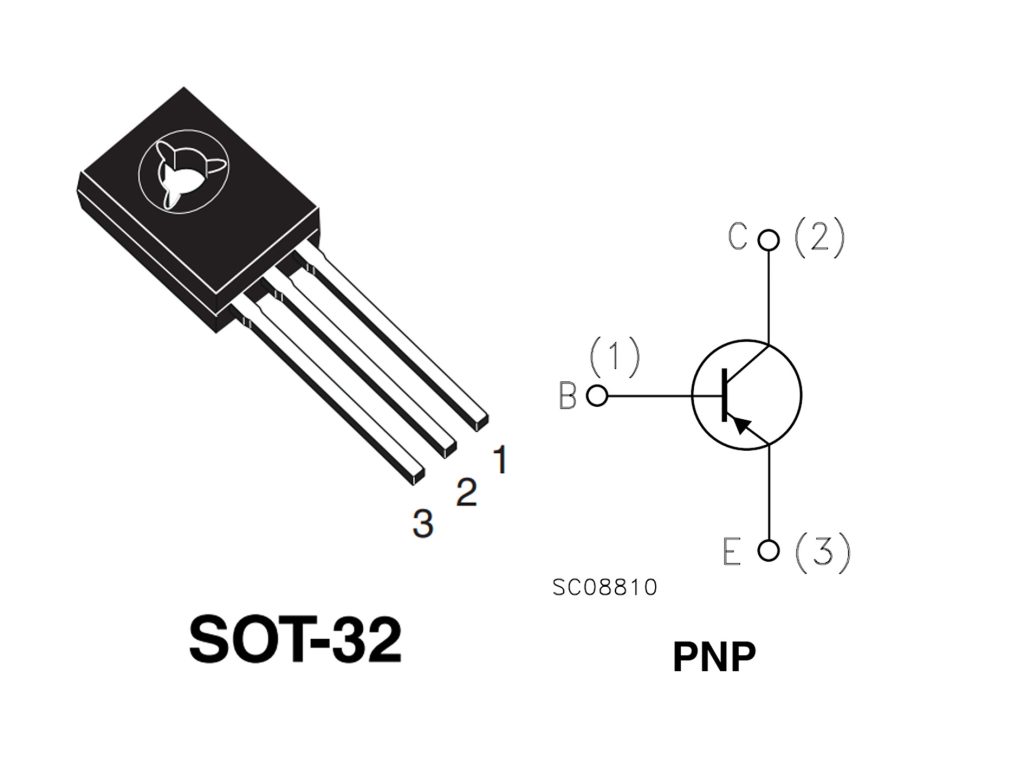
BD140 Pinout Diagram
The BD140 is a PNP transistor commonly used for amplification and switching applications. It features three main terminals: the Base (B), Collector (C), and Emitter (E). The pinout configuration is designed to control the flow of current and manage the transistor’s switching behavior in various electronic circuits.
| Pin Number | Pin Name | Description |
|---|---|---|
| 1 | Base (B) | The base terminal controls the current flow between the collector and emitter. It is used to turn the transistor on or off. |
| 2 | Collector (C) | The collector terminal is where the majority of the current flows through the transistor. It’s connected to the load. |
| 3 | Emitter (E) | The emitter terminal is the output for the current and is connected to the negative side of the circuit. |
In conclusion, the BD140’s pinout configuration is fundamental to its proper functioning in a circuit. The base, collector, and emitter work together to control the current flow, making the transistor ideal for use in power control and amplification tasks.
More Like This

MMBT5550LT1G
onsemi

MMBT2222A
HY Electronic (Cayman) Limited
MMBT3904
HY Electronic (Cayman) Limited
MMBT2907A
HY Electronic (Cayman) Limited

TIP41C
Fairchild Semiconductor

PMBT3904,215
NXP Semiconductors

TIP120
Central Semiconductor Corp

TIP36C
Central Semiconductor Corp
TIP35C
Central Semiconductor Corp

TIP3055
Central Semiconductor Corp
TIP2955
Central Semiconductor Corp
TIP147
Central Semiconductor Corp
Also Add to Cart

SPA11N60C3
Infineon Technologies
.jpg "MMBT5551")
MMBT5551
NTE Electronics, Inc

2SAR573D3TL1
Rohm Semiconductor
BC848CLT1G
onsemi

BCP52-16
STMicroelectronics

TIP35C
onsemi

2N3773
STMicroelectronics

BDW93C
onsemi

2N5551
Fairchild Semiconductor

MMBT5401
MDD
BC847BLT1G
onsemi

MJE3055T
NTE Electronics, Inc
Related Products
MMBT5550LT1G
onsemi
MMBT2222A
HY Electronic (Cayman) Limited
MMBT3904
HY Electronic (Cayman) Limited
MMBT2907A
HY Electronic (Cayman) Limited
TIP41C
Fairchild Semiconductor
PMBT3904,215
NXP Semiconductors
TIP120
Central Semiconductor Corp
TIP36C
Central Semiconductor Corp
TIP35C
Central Semiconductor Corp
TIP3055
Central Semiconductor Corp
TIP2955
Central Semiconductor Corp
TIP147
Central Semiconductor Corp
TIP142
Central Semiconductor Corp

2N2369AUB
Microchip Technology

BCX17
onsemi

BCP69
onsemi
BCP53
onsemi
PZT2907A
onsemi

2SC5200
STMicroelectronics

2N2907A
Micro Commercial Co
BCP52-16
STMicroelectronics

MMBTA92
STMicroelectronics
2N3773
STMicroelectronics
,TO-226_straightlead.jpg "2N5551")
2N5551
onsemi
MPSA92
onsemi
MPS751G
onsemi

MJD44H11
onsemi
MJD127
onsemi

2SC4617
onsemi

TIP42C
onsemi
Please send RFQ , we will respond immediately.
