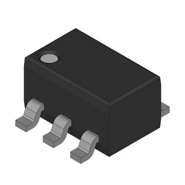
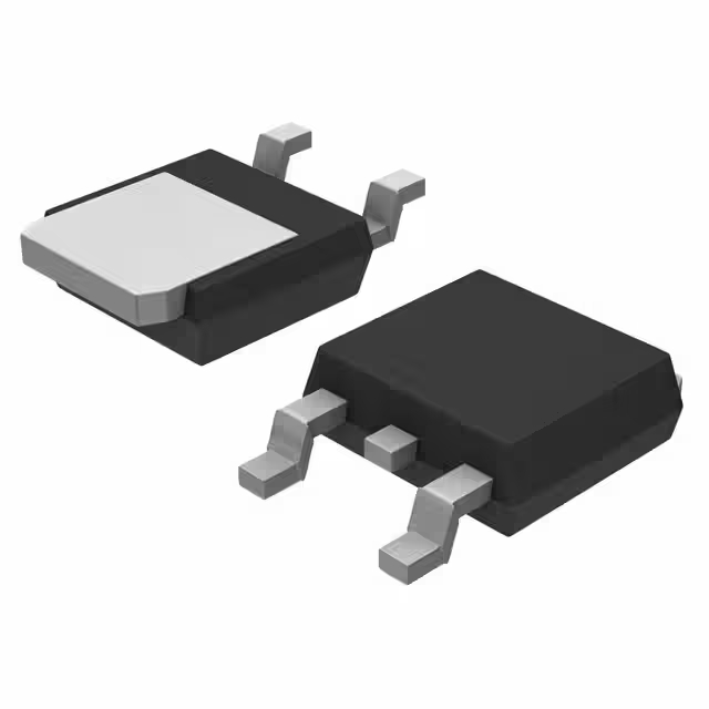
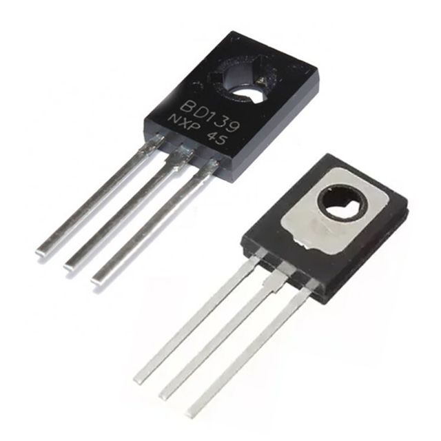
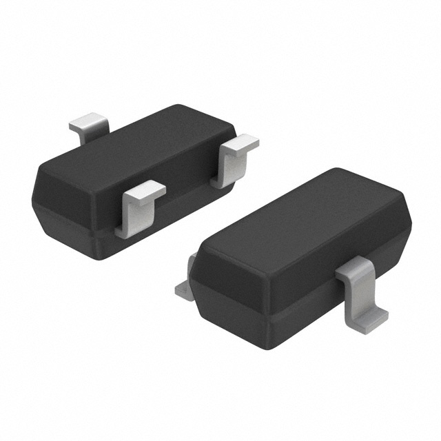
BD139 NPN transistor | Pinout | datasheet | circuit diagram onsemi
- Transistor Type: NPN
- Current-Collector(Ic)(Max): 1.5 A
- Voltage-Collector Emitter Breakdown (Max): 80 V
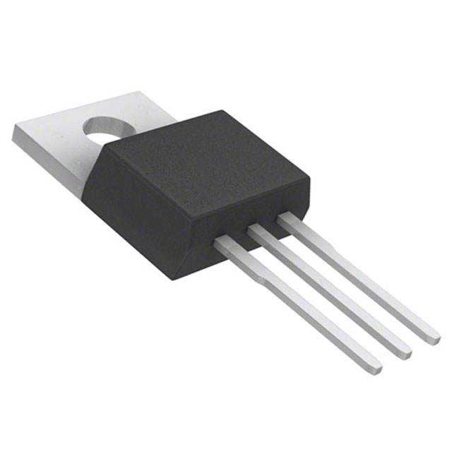
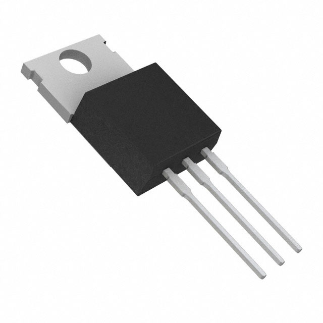
- Package: TO-225AA, TO-126-3

FREE delivery for orders over HK$250.00

Quick response, quick quotaton

Flash shipment,no worries after sales

Original channel,guarantee of the authentic products
bd139 transistor projects ldr sensor
BD139 Switch Circuit
BD139 Introduction
The BD139 is a bipolar medium power NPN transistor (BJT) in a TO-126 package that is primarily used in power amplification circuits, especially low and intermediate frequency amplification circuits. It can withstand high currents and voltages, making it ideal for driving high power loads. It also has a low saturation voltage drop and high switching speed, making it widely used in switching circuits as well. With good temperature characteristics and stability, it maintains reliable performance even under extreme operating conditions.

BD139 Pinout
The amplification range of the BD139 is from 40 to 160, (this is the amplification capability of the BD139). From the datasheet, it can be seen that the current through the collector pin must not exceed 1.5A (if you follow the margin of twenty percent, i.e., it must not exceed 1.5*0.8).
BD139 used as a switch
The following diagram uses a circuit model of BD139 as a switch with a resistor and an LED between the emitter and collector.
When the switch is closed, the transistor BD139 opens and conducts between the collector and emitter as the input is 6V resulting in a current at the base, the current flows through the LED and the LED emits light.
Since there is a PN junction between the base and the emitter, when the base-emitter current increases, the PN junction undergoes forward bias, which in turn leads to an increase in the current between the collector-emitter and the amplification capability of the BD139 is very strong (40 to 160), which enables the BD139 to achieve larger power amplification tasks.

BD139 Switch Circuit







,TO-226_straightlead.jpg)

