
AD9957BSVZ datasheet | price & pdf
- Resolution(Bits): 14 b
- Masterfclk: 1 GHz
- Tuning Word Width(Bits): 32 b
- Package: 100-TQFP Exposed Pad


FREE delivery for orders over HK$250.00

Quick response, quick quotaton

Flash shipment,no worries after sales

Original channel,guarantee of the authentic products

AD9957BSVZ DataSheet — ingketech.net
Download Spain PDF: AD9957BSVZ Datasheet PDF
Download Germany PDF: AD9957BSVZ Datasheet PDF
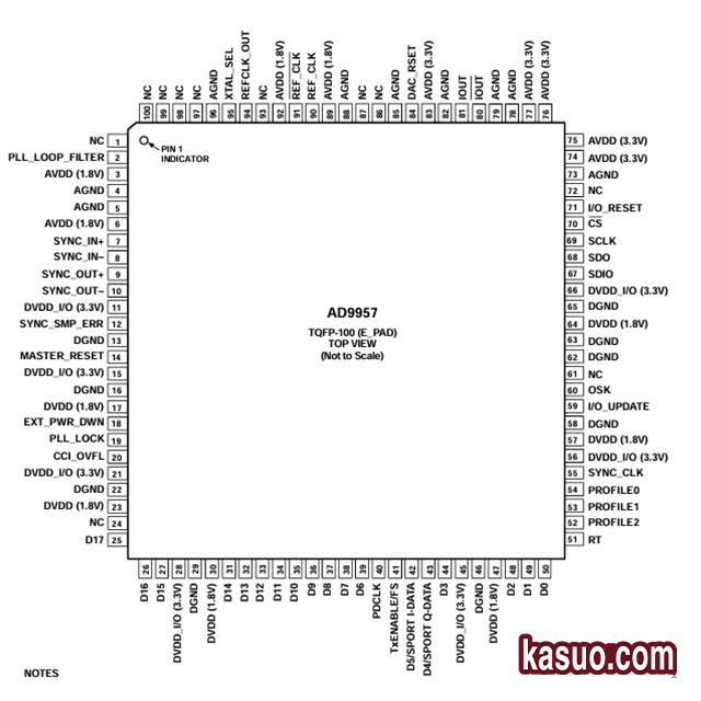
AD9957BSVZ Pinout Equivalent Circuit
The AD9957BSVZ is a high-performance direct digital frequency synthesizer (DDS) from Analog Devices Inc., which integrates a high-speed direct digital frequency synthesizer, a high-precision 14-bit digital-to-analog conversion circuit (DAC), clock circuit, digital filter and DSP arithmetic unit in a single chip. And widely used in communication and frequency measurement and other fields. Because the chip integrates a high-precision digital frequency synthesis circuit, it can be used to generate accurate digital frequency signals, which can meet the high requirements of signal quality and stability in modern communication systems. The user interface is also very convenient, using the Blackfin® DSP SPORT interface.
The AD9957BSVZ is a 100-pin TQFP package with the following main pin types and functions:
Power supply pin:
Analog Power Supply (AVDD) : Provides power to the analog core circuit and DAC portion (including 1.8V and 3.3V).
Digital Power Supply (DVDD) : Provides power to the digital core (1.8V).
Digital I/O power supply (DVDD_I/O) : Provides power to the digital input and output pins (3.3V).
Ground pins (AGND, DGND) : analog ground and digital ground, pay attention to the isolation of the two to prevent interference.
Clock input/output pins:
Reference clock input (REF_CLK, REF_CLK) : Receives external reference clock signals.
Reference clock Output (REFCLK_OUT) : Outputs the reference clock signal.
System Clock Output (SYNC_CLK) : Output system clock signals.
Sync input/output pins:
Synchronization input (SYNC_IN+, SYNC_IN−) : receives an external synchronization signal, with positive rising edge and negative falling edge, and synchronizes the internal clock.
Synchronous output (SYNC_OUT+, SYNC_OUT−) : Output a synchronization signal, which is valid with a positive rising edge and a negative falling edge, to synchronize the external slave clock.
Synchronous sampling error (SYNC_SMP_ERR) : Output of synchronous sampling error, using a digital output, active at a high level.
Control pin
MASTER_RESET: Reset pin, active high, clear all memory device contents, register set to default value.
External Power Saving mode (EXT_PWR_DWN) : Low power pin. When enabled, it works in low power mode.
PLL lock (PLL_LOCK) : Whether the clock multiplier PLL has locked the input to the reference clock.
Data input/output pins:
Parallel data input (D[17:0]) : Parallel data input bus, active at high level, to complete up-conversion processing.
Serial Data Input/Output (SDIO) : Serial data input/output pin for serial data transmission.
Serial Data Output (SDO) : Serial data output pin, valid only in unidirectional serial data mode.
Serial Data Clock (SCLK) : Controls the timing of serial data transfer.
Slice Selection (CS) : low active, enabling serial data transfer.
Configuration pin:
PROFILE selection (PROFILE<2:0>) : Used to select phase and frequency profile pins for the DDS kernel.
Input/Output update (I/O_UPDATE) : The update pin of the data input or output, active at a high level, indicates that the I/O cache will be transferred to the appropriate register.
Output shift keying (OSK) : Controls the output shift keying function, and the digital input is active at a high level.
RAM trigger (RT) : The operating pin that controls the RAM, active at high level.
Analog output pin:
DAC Output (IOUT) : DAC output current source, analog output, connected to ground via an external resistor (50Ω).
DAC Reference Setting (DAC_RSET) : Sets the full-scale reference current of the DAC output.
Alternative model selection:
When looking for alternatives TO the AD9957BSVZ, there are several points to note, such as frequency range, resolution, and operating power supply voltage, etc. This article will introduce several similar products, but not 100% PIN TO PIN available.
AD9954YSVZ: Frequency range up to 400MHz, resolution of 14 bits, supply voltage of 3.3V and 1.8V; The main application scenarios are medium frequency and device size limited applications.
AD9958BCPZ: The AD9958BCPZ has a frequency range of up to 500MHZ, a resolution of 10 bits, and a supply voltage of 3.3V and 1.8V. It is mainly used in scenarios where the resolution is not very high but high frequency output is required

AD9910BSVZ: The AD9910BSVZ has a frequency range of up to 1Ghz, a resolution of 14 bits, and a supply voltage of 3.3V and 1.8V. It is basically the same as the AD9957BSVZ, but it is higher in frequency and resolution than the AD9957BSVZ, which is suitable for scenes requiring high frequency output and high resolution.

Application scenario:
The diagram shows the circuit diagram of the AD9557 simulator, which uses the AD9557 analog output and connects with the virtual oscilloscope and spectrograph, mainly including the following modules.
The AD9557 module has a direct digital frequency synthesizer unit, which is responsible for generating analog signals with adjustable frequency and amplitude and generating output signals to the oscilloscope or spectrometer through the DAC circuit;
Scaling components. The two paths in the figure both contain DAC_LOAD_SCALE and DAC_LOAD_THEV, which adjust the amplitude of the output signal by pull-down resistance and other characteristics, through which different measurement requirements can be used.
The oscilloscope and spectrum analyzer can view the time domain waveform of the signal and analyze the frequency domain composition of the signal.
Application drawing

More Like This

74HCT280D,653
NXP USA Inc.

74HCT280N,652
NXP USA Inc.
N74F280BN,602
NXP USA Inc.

1621B2UZZGR
Texas Instruments
1621B1UZZGR
Texas Instruments

SN74S280NSRG4
Texas Instruments

SN74LS280DRG4
Texas Instruments
SN74AS286NSRG4
Texas Instruments
SN74AS286DRG4
Texas Instruments
SN74AS280DRG4
Texas Instruments
SN74ALS280DRG4
Texas Instruments
SN74ALS280DG4
Texas Instruments
Also Add to Cart

TPS7A3001DRBR
Texas Instruments

DSPIC33EP256MU810-I/PT
Microchip Technology

VN5E160ASTR-E
STMicroelectronics

DRV8876RGTR
Texas Instruments

MC908AZ60ACFU
Motorola

GL850G-OHY37
Genesys Logic

NCV8406BDTRKG
onsemi

STM32F103ZFT6
STMicroelectronics
AD737JRZ
Analog Devices Inc.
24AA02E48T-I/SN
Microchip Technology

CD14538BM96
Texas Instruments

LM3480IM3X-3.3
National Semiconductor
Related Products
74HCT280D,653
NXP USA Inc.
74HCT280N,652
NXP USA Inc.
N74F280BN,602
NXP USA Inc.
1621B2UZZGR
Texas Instruments
1621B1UZZGR
Texas Instruments
SN74S280NSRG4
Texas Instruments
SN74LS280DRG4
Texas Instruments
SN74AS286NSRG4
Texas Instruments
SN74AS286DRG4
Texas Instruments
SN74AS280DRG4
Texas Instruments
SN74ALS280DRG4
Texas Instruments
SN74ALS280DG4
Texas Instruments

CY74FCT480BTSOCTG4
Texas Instruments
CD74AC280M96G4
Texas Instruments
74ACT11286NG4
Texas Instruments
74ACT11286N
Texas Instruments

SY10E193JZ TR
Microchip Technology
SY10E193JZ
Microchip Technology
SY10E160JZ TR
Microchip Technology
SY10E160JZ
Microchip Technology
SY100S360JZ-TR
Microchip Technology
SY100S360JZ
Microchip Technology
SY100E193JZ TR
Microchip Technology
SY100E193JZ
Microchip Technology
SY100E160JZ TR
Microchip Technology
SY100E160JZ
Microchip Technology
SN74S280NSRE4
Texas Instruments
SN74S280NSR
Texas Instruments
SN74LS280DRE4
Texas Instruments
SN74LS280DR
Texas Instruments