AD9914BCPZ datasheet, price & pdf
- Resolution(Bits): 12 b
- Masterfclk: -
- Tuning Word Width(Bits): -
- Package: 88-VFQFN Exposed Pad, CSP

AD9914BCPZ Analog Devices Datasheet
AD9914bcpz Pinout Equivalent Circuit

AD9914bcpz is a high-performance direct digital synthesizer produced by Analog Devices. It adopts advanced digital signal synthesis technology and is equipped with a 3.5-GSPS high-speed clock and a 12 bit high-precision DAC, which can achieve 16 bit phase fine-tuning and 12 bit amplitude control. It has programmable analog-to-digital function and automatic linear and nonlinear frequency scanning function. At 1396 MHz with a 1 kHz offset, ultra-low phase noise of -128 dBc/Hz can be achieved, while maintaining broadband SFDR below -50 dBc. Adopting 1.8V/3.3V dual power supply and providing software and hardware dual shutdown function; The built-in PLL REF CLK multiplier further enhances clock stability.
AD9914bcpz adopts LFCSP-88 (12×12) package, and the specific pin definitions are as follows:
| Pin No. | Name | Description |
|---|---|---|
| 1, 2, 13 to 15, 68 to 72, 75 to 81, 87, 88 | D5 to D7, D16 to D31, D27 to D31 | Parallel port pins. The 32-bit parallel port provides options for serial or parallel programming of internal registers. |
| 3 | D15/A7 | Parallel port pins/address lines. The state of F0 to F3 determines whether this pin is used for direct FSK, PSK, or ASK data, or as an address line for programming internal registers. |
| 4 | D14/A6 | Parallel port pins/address lines. The state of F0 to F3 determines whether this pin is used for direct FSK, PSK, or ASK data, or as an address line for programming internal registers. |
| 5 | D13/A5 | Parallel port pins/address lines. The state of F0 to F3 determines whether this pin is used for direct FSK, PSK, or ASK data, or as an address line for programming internal registers. |
| 8 | D12/A4 | Parallel port pins/address lines. The state of F0 to F3 determines whether this pin is used for direct FSK, PSK, or ASK data, or as an address line for programming internal registers. |
| 9 | D11/A3 | Parallel port pins/address lines. The state of F0 to F3 determines whether this pin is used for direct FSK, PSK, or ASK data, or as an address line for programming internal registers. |
| 10 | D10/A2 | Parallel port pins/address lines. The state of F0 to F3 determines whether this pin is used for direct FSK, PSK, or ASK data, or as an address line for programming internal registers. |
| 11 | D9/A1 | Parallel port pins/address lines. The state of F0 to F3 determines whether this pin is used for direct FSK, PSK, or ASK data, or as an address line for programming internal registers. |
| 12 | D8/A0 | Parallel port pins/address lines. Enable serial mode, this pin is used to reset the serial port. |
| 18 | D4/SYNCIO | Parallel port pin/serial port synchronization pin. Enable serial mode, this pin is used for the read back mode of serial operation. |
| 19 | D3/SDO | Parallel port pins/serial data output. Serial mode: This pin is used for SDIO serial operation. Parallel mode, this pin is used for writing operations to update internal registers. |
| 20 | D2/SDIO/WR | Parallel port pins/serial data input/output/write input. |
| 21 | D1/SCLK/RD | Parallel port pins/serial clock/read input. If serial mode is enabled, this pin is used for SCLK for serial operation. If parallel mode is enabled, it is used for read operations to read internal registers |
| 22 | DO/CS/PWD | Parallel port pin/chip selection/parallel width. Enable serial mode for chip selection for serial operations. Enable parallel mode for setting 8-bit or 16 bit data. |
| 6, 23, 73 | DVDD (1.8V) | Digital power supply (1.8V). |
| 7, 17, 24, 74, 84 | DGND | Digitally speaking. |
| 16, 83 | DVDD_I/O (3.3V) | Digital input/output power supply (3.3V). |
| 32, 56, 57 | AVDD (1.8V) | Simulate core power supply (1.8V). |
| 33, 35, 37, 38, 44, 46, 49, 51 | AGND | Simulated ground. |
| 34, 36, 39, 40, 43, 47, 50, 52, 53, 60 | AVDD (3.3V) | Analog DAC power supply (3.3V). |
| 25, 26, 27 | PSO to PS2 | Select pins for the configuration file. Digital input (high level valid). The state change must be set at the rising edge of the SYNC CLK pin (pin 82). |
| 28, 29, 30, 31 | FO to F3 | Functional pins. Digital input. The status of these pins determines whether to use a serial or parallel interface. It also decides how to partition 32-bit parallel data words for FSK, PSK, or ASK modulation modes. |
| 41 | AOUT | DAC complementary output source. Analog signal output. Internally connected to AVDD (3.3V) through a 50 Ω resistor. |
| 42 | AOUT | DAC output source. Analog signal output. Internally connected to AVDD (3.3V) through a 50 Ω resistor |
| 45 | DAC_BP | DAC bypass pin. Grounding capacitors can improve the noise performance of DAC output. |
| 48 | DAC_RSET | Simulated reference. Connect to AGND through a 3.3k Ω resistor. |
| 54 | Complementary reference clock input. Simulate input. | |
| 55 | REF_CLK | Reference clock input. Simulate input. |
| 58 | LOOP_FILTER | External PLL loop filter node. |
| 59 | REF | Local PLL reference power supply. Generally, it is 2.05V. |
| 61 | SYNC_OUT | Digital synchronous output. Clock source (output) used to synchronize multiple chips. |
| 62 | SYNC_IN | Digital synchronous input. Clock receiver (input) used for synchronizing multiple chips. |
| 63 | DRCTL | Slope control. Digital input (high level valid). This pin controls the scanning direction. |
| 64 | DRHOLD | Slope maintenance. Digital input (high level valid). Pause scanning upon activation. |
| 65 | DROVER | The slope ends. Digital output (high level effective). |
| 66 | OSK | Output shift key control. Digital input (high level valid). Only valid when enabled through register bits. |
| 67 | EXT_PWR_DWN | External power is turned off. Digital input (high level valid). |
| 82 | SYNC_CLK | Clock output. Many digital inputs on the chip (parallel data ports (DO to D31)) must be configured on the rising edge of this signal. |
| 85 | MASTER_RESET | Master reset. Digital input (high level valid). Clear all storage elements and set the registers to default values. |
| 86 | I/O_UPDATE | Input/output updates. Digital input (high level valid). Transfer the contents of the input/output buffer to the corresponding internal register under high voltage conditions. |
| EPAD | Exposed Pad | EPAD must be welded to the ground. |
Alternative chip selection
In hardware system design, when searching for alternative devices for AD9914BCPZ due to supply, cost, or special application requirements, the key parameters to consider are as follows: the first alternative chip needs to cover the frequency band required by the target system (if the frequency band can be reduced, lower level alternatives can be selected); The second requirement is to have high resolution, low phase noise, and multiple modulation functions similar to AD9914; The third is to ensure that the substitute products are compatible with SPI communication interfaces and packaging forms, so that there is no need to redesign the PCB and the product can be modified faster.
| Picture | Name | Supply voltage | Resolution | Slew rate | Package |
|---|---|---|---|---|---|
 |
AD9914S | 1.8V/3.3V | 12 | 3.5 GSPS | LFCSP-88 (12×12) |
 |
AD9915 | 1.8V/3.3V | 12 | 2.5 GSPS | LFCSP-88 (12×12) |
 |
AD9912ABCPZ | 1.8V/3.3V | 12 | 1 GSPS | LFCSP-64 (9×9) |
Typical applications of AD9914BCPZ
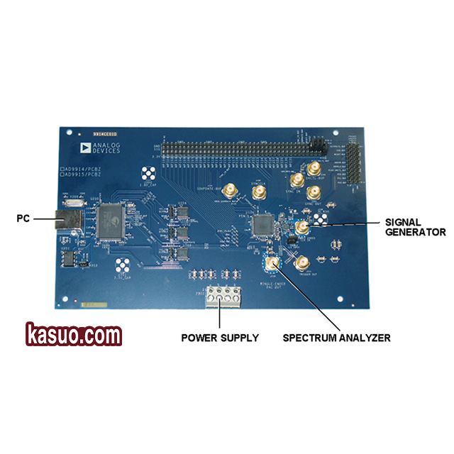
The figure shows a circuit board (PCB) manufactured by Analog Devices for verifying AD9914bcpz, specifically designed for high-precision signal processing. Multiple key components are integrated on the PCB, including multi pin header connectors, SMA connectors, USB interfaces, and power conversion modules. The top connector is used for external devices or expanding I/O connections; The SMA connectors on the right are connected to the “signal generator” and “spectrum analyzer” respectively, used to view the output of the signal; The power conversion module at the bottom is connected to an external power supply through screw terminals; The USB interface on the left is a port for communication with a PC, used to connect to a computer and achieve functions such as control and data acquisition. The overall design meets the requirements of the vast majority of experiments and is suitable for research in fields such as radio frequency and communication engineering.
More Like This

74HC573D
Toshiba Semiconductor and Storage
74HC373D
NXP USA Inc.

CD4043BE
Harris Corporation

SN74HC573NSR
Texas Instruments

SN74ALVCH16373DGGR
Texas Instruments

SN74HC573ADW
Texas Instruments

SN74AC573PWR
Texas Instruments

SN74LS373N
Texas Instruments
SN74HCT373N
Texas Instruments

CD4043BE
Texas Instruments

SN74HC259N
Texas Instruments
SN74LVC16373ADGGR
Texas Instruments
Also Add to Cart

TPS23754PWP
Texas Instruments

AD8691AUJZ-REEL7
Analog Devices Inc.

TPS7A4501KTTR
Texas Instruments

MX25L25645GM2I-08G
Macronix

74VHC595MX
Fairchild Semiconductor

CD4052BE
Texas Instruments

HMC1060LP3ETR
Analog Devices Inc.

IPW65R045C7
Infineon Technologies

TMS320F241PGS
Texas Instruments

5M160ZE64A5N
Intel

NBA3N012CSNT1G
onsemi

EP3C40F484I7
Intel
74HC573D
Toshiba Semiconductor and Storage
74HC373D
NXP USA Inc.
CD4043BE
Harris Corporation
SN74HC573NSR
Texas Instruments
SN74ALVCH16373DGGR
Texas Instruments
SN74HC573ADW
Texas Instruments
SN74AC573PWR
Texas Instruments
SN74LS373N
Texas Instruments
SN74HCT373N
Texas Instruments
CD4043BE
Texas Instruments