AD9858BSVZ Datasheet & Pricing Information
- Resolution(Bits): 10 b
- Masterfclk: 1 GHz
- Tuning Word Width(Bits): 32 b
- Package: 100-TQFP Exposed Pad

AD9858BSVZ Analog Devices Datasheet-INGKECHIPS.COM
Download Japanese PDF: AD9858BSVZ Datasheet PDF
AD9858BSVZ Pinout Equivalent Circuit
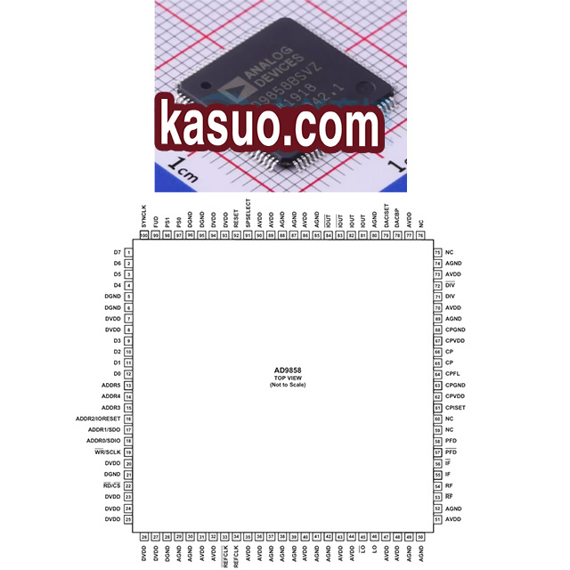
AD9858BSVZ is a 1 GSPS direct digital synthesizer chip from Analog Devices, which has the advantages of high resolution, fast frequency switching and low phase noise, and is one of the representative products of the new generation of frequency synthesizers. It integrates a 10-bit high-speed digital-to-analog converter (DAC), phase accumulator, sine wave look-up table, and programmable frequency registers to form a complete DDS, as well as an on-chip phase-locked loop (PLL) that multiplies the system clock and increases the output frequency range.
AD9858BSVZ With internal clock speeds up to 1 GSPS, system clock frequencies up to 2GHz with internal PLL multipliers, excellent phase noise and SFDR, frequency scaling resolution up to 48 bits, and low power consumption (2W typical) to meet the vast majority of high-precision frequency synthesis needs.
Pin Definition:
| Pin No. | Mnemonic | I/O | Description |
|---|---|---|---|
| 1 to 4, 9 to 12 | D7 to D0 | I | Parallel Port Data. The functionality of these pins is valid only when the I/O port is configured as a parallel port. |
| 5, 6, 21, 28, 95, 96 | DGND | Digital Ground. | |
| 7, 8, 20, 23 to 27, 93, 94 | DVDD | Digital Supply Voltage. | |
| 13 to 18 | ADDR5 to ADDR0 | I | When the I/O port is configured as a parallel port, these pins serve as a 6-bit address select for accessing the on-chip registers (see the IORESET, SDO, and SDIO pins for the serial port mode). |
| 16 | IORESET | I | Valid for serial programming mode only. Resets the serial I/O bus controller. Used for recovery from unresponsive serial bus due to improper programming protocol. |
| 17 | SDO | O | Valid for serial programming mode only. In 3-wire mode, this is a unidirectional serial data output. In 2-wire mode, unused. |
| 18 | SDIO | I/O | Valid for serial programming mode only. In 3-wire mode, this is the serial data input. In 2-wire mode, it is a bidirectional serial data pin. |
| 19 | WR/SCLK | I | In parallel mode: active low write pulse (WR). In serial mode: serial data clock (SCLK). |
| 22 | RD/CS | I | In parallel mode: active low read pulse (RD). In serial mode: active low chip select (CS) for device selection. |
| 29, 30, 37 to 39, 41, 42, 49, 50, 52, 69, 74, 80, 85, 87, 88 | AGND | I | Analog Ground. |
| 31, 32, 35, 36, 40, 43, 44, 47, 48, 51, 70, 73, 77, 86, 89, 90 | AVDD | I | Analog Supply Voltage. |
| 33 | REFCLK | I | Reference Clock Complementary Input. When the REFCLK port operates in single-ended mode, REFCLK should be decoupled to AVDD with a 0.1 µF capacitor. |
| 34 | REFCLK | I | Reference Clock Input. |
| 45 | LO | I | Mixer Local Oscillator (LO) Complementary Input. When the LO port operates in single-ended mode, LO should be decoupled to AVDD with a 0.1 µF capacitor. |
| 46 | LO | I | Mixer Local Oscillator (LO) Input. |
| 53 | RF | I | Analog Mixer RF Complementary Input. When the RF port operates in single-ended mode, RF should be decoupled to AVDD with a 0.1 µF capacitor. |
| 54 | RF | I | Analog Mixer RF Input. |
| 55 | IF | O | Analog Mixer IF Output. |
| 56 | IF | O | Analog Mixer IF Complementary Output. |
| 57 | PFD | I | Phase Frequency Detector Complementary Input. When the PFD port operates in single-ended mode, PFD should be decoupled to AVDD with a 0.1 µF capacitor. |
| 58 | PFD | I | Phase Frequency Detector Input. |
| 59, 60, 75, 76 | NC | No Connection. | |
| 61 | CPISET | I | Charge Pump Output Current Control. A resistor connected from CPISET to CPGND establishes the reference current for the charge pump. |
| 62, 67 | CPVDD | I | Charge Pump Supply Voltage. |
| 63, 68 | CPGND | I | Charge Pump Ground. |
| 64 | CPFL | O | Charge Pump Fast Lock Output. |
| 65, 66 | CP | O | Charge Pump Output. |
| 71 | DIV | I | Phase Frequency Detector Feedback Input. |
| 72 | DIV | I | Phase Frequency Detector Feedback Complementary Input. When the DIV port operates in single-ended mode, DIV should be decoupled to AVDD with a 0.1 µF capacitor. |
| 78 | DACBP | DAC Baseline Decoupling Pin. Typically bypassed to Pin 77 with a 0.1 µF capacitor. | |
| 79 | DACISET | I | A resistor connected from DACISET to AGND establishes the reference current for the DAC. |
| 81, 82 | IOUT | O | DAC Output. |
| 83, 84 | IOUT | O | DAC Complementary Output. |
| 91 | SPSELECT | I | I/O Port Serial/Parallel Programming Mode Select Pin. Logic 0 is serial programming mode, and Logic 1 is parallel programming mode. |
| 92 | RESET | I | Active High Hardware Reset Pin. Assertion of the RESET pin forces the AD9858 to its default operating conditions. |
| 97, 98 | PS0, PS1 | I | Used to select one of the four internal profiles. These pins are synchronous to the SYNCLK output. |
| 99 | FUD | I | Frequency Update. The rising edge transfers the contents of the internal buffer registers to the memory registers. This pin is synchronous to the SYNCLK output. |
| 100 | SYNCLK / EPAD | O | Clock Output Pin. Serves as a synchronizer for external hardware. SYNCLK runs at REFCLK/8. Exposed paddle must be soldered to ground. |
Alternative Model Options:
Substitutes that are identical to the AD9858BSVZ and functionally equivalent are rare, so we focus more on devices with similar functions or consistent packages during the selection process. These alternatives are partially similar in terms of frequency resolution, power consumption levels, control interface types, and package formats, but do not have full pin compatibility or functional consistency. The following alternative selection suggestions are based on the principle of “partially compatible with functions”.
| Picture | Name | Operating Voltage | Highest System Clock Frequency | Frequency Resolution | Package |
|---|---|---|---|---|---|
 |
AD9957BSVZ-REEL | 1.8V~3.3V | 1GHz | 14 | TQFP-100-EP (14×14) |
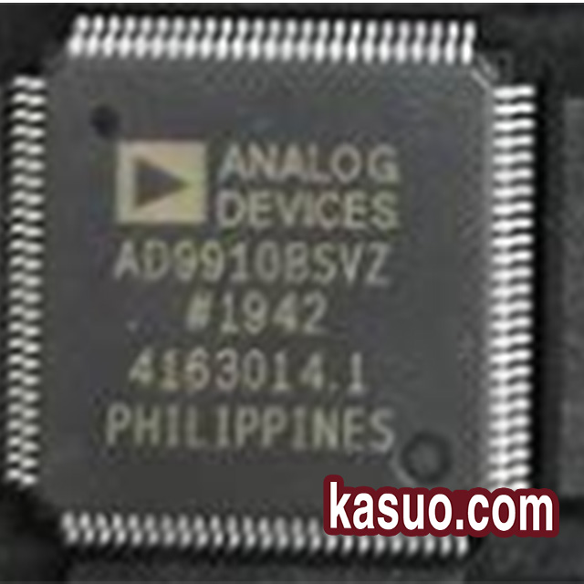 |
AD9910BSVZ-REEL | 1.8V~3.3V | 1GHz | 14 | TQFP-100-EP (14×14) |
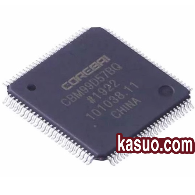 |
CBM99D57BQ | 1.8V~3.3V | 1GHz | 14 | TQFP-100-EP (14×14) |
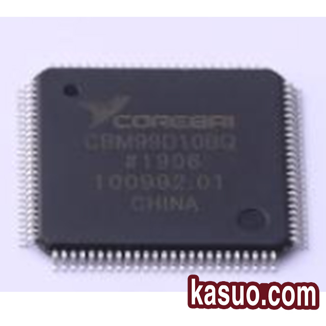 |
CBM99D10BQ | 1.8V~3.3V | 1GHz | 14 | TQFP-100-EP (14×14) |
Typical Applications:

The figure shows a DDS-based variable frequency loop oscillator, which provides digital control to achieve high accuracy frequency signals. The specific process is as follows: the input first enters a 1GSPS DDS module to generate a high-resolution digital signal; Next, it is divided into two channels, one of which is directly converted into analog signal through the DAC and removed by the DC-400 MHz low-pass filter, and the other is generated by the frequency divider to generate a fixed loop LO1 to provide a stable 2GHz local oscillator signal to ensure the mixing accuracy. After that, the signal enters the PLL loop, the frequency is reduced by a programmable divider (÷2/÷4), and compared with the reference frequency in a 150MHz phase detector, the error signal generated is converted into a stable voltage by the charge pump (0.5mA~2mA adjustable) and the loop filter, and the VCO is controlled to output an oscillation signal of 2GHz±150 MHz. The system supports frequency synthesis over a wide range and low phase noise by combining the high resolution of DDS with the stability of the PLL, making it suitable for scenarios where frequency accuracy is critical, such as communication systems, radars, and test instruments.
More Like This

74HC573D
Toshiba Semiconductor and Storage
74HC373D
NXP USA Inc.

CD4043BE
Harris Corporation

SN74HC573NSR
Texas Instruments

SN74ALVCH16373DGGR
Texas Instruments

SN74HC573ADW
Texas Instruments

SN74AC573PWR
Texas Instruments

SN74LS373N
Texas Instruments
SN74HCT373N
Texas Instruments

CD4043BE
Texas Instruments

SN74HC259N
Texas Instruments
SN74LVC16373ADGGR
Texas Instruments
Also Add to Cart

LM5022QDGSRQ1
Texas Instruments

AD8044AR-14
Analog Devices Inc.

ADM3490EARZ
Analog Devices Inc.

ADS8568SPM
Texas Instruments
LM5069MM-2/NOPB
Texas Instruments

LTC3350EUHF
Analog Devices Inc.

DRV110APWR
Texas Instruments

ATMEGA88PA-MUR
Atmel

SP3072EEN-L/TR
MaxLinear, Inc.

SE555D
Texas Instruments

TS912ID
STMicroelectronics
SN74HC574NSR
Texas Instruments
74HC573D
Toshiba Semiconductor and Storage
74HC373D
NXP USA Inc.
CD4043BE
Harris Corporation
SN74HC573NSR
Texas Instruments
SN74ALVCH16373DGGR
Texas Instruments
SN74HC573ADW
Texas Instruments
SN74AC573PWR
Texas Instruments
SN74LS373N
Texas Instruments
SN74HCT373N
Texas Instruments
CD4043BE
Texas Instruments