
AD9833BRMZ-REEL7 | Datasheet & Price
- Resolution(Bits): 10 b
- Masterfclk: 25 MHz
- Tuning Word Width(Bits): 28 b
- Package: 10-TFSOP, 10-MSOP (0.118, 3.00mm Width)


FREE delivery for orders over HK$250.00

Quick response, quick quotaton

Flash shipment,no worries after sales

Original channel,guarantee of the authentic products
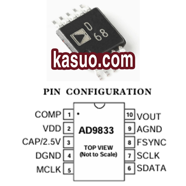
AD9833BRMZ-REEL7 Pinout Equivalent Circuit
AD9833BRMZ-REEL7 is a low-power programmable waveform generator designed by Analog Devices. Key features include a wide output frequency range (0 MHz to 12.5 MHz), 28-bit resolution, no external components, and a 3-wire SPI interface. It can generate digital signals of different frequencies and phases, and is mainly used for frequency synthesis, waveform generation, and test signal generation. Due to its high resolution and lack of external circuits, it is widely used in communication equipment, audio generation, clock signal generation, and other fields.
The AD9833BRMZ-REEL7 is available in an MSOP-10 package with the following pin functions:
| Pin number | Pin name | Description of the function |
|---|---|---|
| 1 | COMP | DAC bias pin to decouple the paranoid voltage of the DAC. |
| 2 | VDD | The power supply pin, connected to a +3.3V or ±5V supply, provides the operating voltage to the chip. |
| 3 | CAP/2.5V | The bit-to-digital circuit provides a stable 2.5V voltage when the VDD input is greater than 2.7V. |
| 4 | DGND | Digital ground. |
| 5 | MCLK | Digital clock input pin. |
| 6 | SDATA | Serial data input pins. |
| 7 | SCLK | Serial clock input, data is passed in on the falling edge. |
| 8 | FSYNC | Active low control input, frame synchronization signal of input data. |
| 9 | AGND | Simulate ground. |
| 10 | VOUT | Signal output pins for outputting analog and digital signals. |
Alternative model selection:
It is rare to find a replacement product that is exactly the same as the AD9833BRMZ-REEL7 model, so we can only find a similar function, such as the AD9833BRMZ-REEL7 in terms of resolution, power consumption, interface type and package. Therefore, for the following alternative selection, I will adopt a partially compatible form.
| Picture | Name | Operating Voltage | Resolution | Clock Frequency | Package |
|---|---|---|---|---|---|
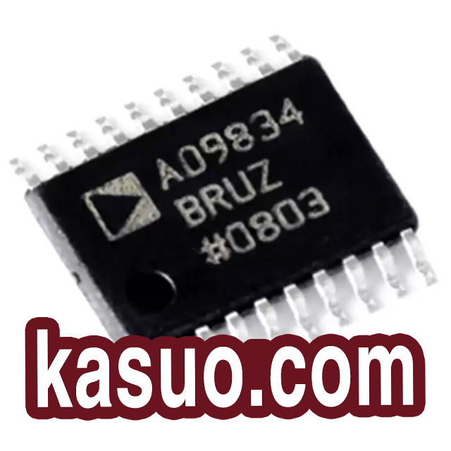 |
AD9834BRUZ-REEL | 2.3V ~ 5.5V | 10 | 75MHz | TSSOP-20 |
 |
AD9833WBRMZ-REEL | 2.3V ~ 5.5V | 10 | 25MHz | MSOP-10 |
 |
AD9837BCPZ-RL7 | 2.3V ~ 5.5V | 10 | 16MHz | LFCSP-10 (3×3) |
 |
AD9851BRSZRL | 2.7V ~ 5.25V | 10 | 180MHz | SSOP-28-208mil |
 |
AD9832BRUZ-REEL7 | 2.97V ~ 5.5V | 10 | 25MHz | TSSOP-16 |
Typical Applications:

Due to the high level of integration of the AD9833BRMZ-REEL7, only a small number of peripheral components are needed to make a generator that supports sine wave, square wave and other waveforms, and the specific hardware is shown in the figure. The diagram contains a voltage regulator that provides voltage to the chip, and a crystal oscillator that provides the clock to the chip. With the help of Analog Devices’ Sweep software, we can configure the input waveform through the SPI protocol to control the hardware output different waveforms.
In the hardware design, it is first necessary to provide a stable supply voltage (2.3V to 5.5V) and ensure the stability of the clock source (MCLK) provided by the external crystal oscillator to ensure the accuracy of the output signal. When communicating with the host computer,you need to pay attention to level matching. The output signal pins should be selectively filtered with capacitors to reduce noise. When laying out the PCB, pay attention to separating the analog and digital grounds, and minimize the high-frequency signal. It is mainly necessary to refer to the application manual of the chip for the design of hardware circuits.
More Like This

BQ48SH-28X6NSH
Texas Instruments

DS9034PCI
Analog Devices Inc./Maxim Integrated
DS90340I-PCX
Analog Devices Inc./Maxim Integrated
DS1260-50
Analog Devices Inc./Maxim Integrated
DS1260-25
Analog Devices Inc./Maxim Integrated
DS1260-100
Analog Devices Inc./Maxim Integrated
DS9034PC
Analog Devices Inc./Maxim Integrated
DS9034PCX
Analog Devices Inc./Maxim Integrated

M4Z28-BR00SH1
STMicroelectronics

DS9034I-PCX+
Analog Devices Inc./Maxim Integrated
DS9034PCI+
Analog Devices Inc./Maxim Integrated
DS9034PCX+
Analog Devices Inc./Maxim Integrated
Also Add to Cart

DS1307Z+
Analog Devices Inc./Maxim Integrated

IS25LP512M-RMLE
ISSI, Integrated Silicon Solution Inc

TLE2074IDWR
Texas Instruments
HEF4047BT
Nexperia

MPC8308CVMAGDA
NXP USA Inc.

STM32F765VIT6
STMicroelectronics
LPC1549JBD100
NXP Semiconductors

TPS22946YZPR
Texas Instruments

XCKU060-1FFVA1517I
AMD Xilinx

ATMEGA16A-MU
Microchip Technology
MAX485MJA
Analog Devices Inc./Maxim Integrated

RS2118YUTQK10
Jiangsu RUNIC Tech
Related Products
BQ48SH-28X6NSH
Texas Instruments
DS9034PCI
Analog Devices Inc./Maxim Integrated
DS90340I-PCX
Analog Devices Inc./Maxim Integrated
DS1260-50
Analog Devices Inc./Maxim Integrated
DS1260-25
Analog Devices Inc./Maxim Integrated
DS1260-100
Analog Devices Inc./Maxim Integrated
DS9034PC
Analog Devices Inc./Maxim Integrated
DS9034PCX
Analog Devices Inc./Maxim Integrated
M4Z28-BR00SH1
STMicroelectronics
DS9034I-PCX+
Analog Devices Inc./Maxim Integrated
DS9034PCI+
Analog Devices Inc./Maxim Integrated
DS9034PCX+
Analog Devices Inc./Maxim Integrated
DS9034PC+
Analog Devices Inc./Maxim Integrated
EPXA4XXA
Intel

EPXA4F672C3GZ
Intel
EPXA4F672C1GZ
Intel
EPXA4F672I2
Intel
EPXA4F672C3
Intel
EPXA4F672C2ES
Intel
EPXA4F672C2
Intel
EPXA4F672C1ES
Intel
EPXA4F672C1
Intel

EPXA4F1020C3
Intel
EPXA4F1020C2ES
Intel
EPXA4F1020C2
Intel
EPXA4F1020C1ES
Intel
EPXA4F1020C1
Intel
EPXA1F672C3
Intel
EPXA1F672C2ES
Intel
EPXA1F672C1ES
Intel
Please send RFQ , we will respond immediately.
