
NC7WZ17P6X datasheet | price, pdf onsemi
- Tipo de lógica: Buffer, Non-Inverting
- Número de elementos: 2
- Número de bits por elemento: 1
- Paquete: 6-TSSOP, SC-88, SOT-363


Envío GRATUITO para pedidos superiores a HK$250.00

Respuesta rápida, cotización rápida.

Envío rápido, sin preocupaciones posventa.

Canal original, garantía de los productos auténticos.
nc7wz17p6x
If you’re working with digital circuits, the NC7WZ17P6X is a handy little Schmitt Trigger buffer you’ll want to keep in mind. It’s especially useful because it can clean up noisy input signals, meaning even if your input fluctuates slowly or is noisy, your output stays stable.
It’s great for battery-powered projects or portable gadgets, as it runs smoothly between 1.65V to 5.5V. Plus, it has a strong output drive, so you won’t need extra circuitry to handle multiple logic inputs or heavier loads.
Speed-wise, it’s impressive, delivering signals within just a few nanoseconds, ideal for fast-paced data communications or digital signal tasks. Despite its speed, it remains power-efficient, keeping your battery life nice and long.
Its ultra-tiny SC-70 (SOT-363) package makes it a perfect fit for wearables, small consumer electronics, or compact PCB layouts, helping you maximize your space effectively.
nc7wz17p6x pinout diagram
| Número PIN | Nombre del pin | Descripción |
|---|---|---|
| 1 | A1 | Channel 1 input, Schmitt trigger input |
| 2 | Tierra | Suelo |
| 3 | A2 | Channel 2 input, Schmitt trigger input |
| 4 | Y2 | Channel 2 output, buffered output |
| 5 | VCC | Power supply input (1.65~5.5V) |
| 6 | Y1 | Channel 1 output, buffered output |
When setting up the NC7WZ17P6X, keep in mind a few helpful tips to make things go smoothly. First off, those Schmitt Trigger inputs (pins A1 and A2) are great at handling noisy or slowly changing signals. Just be sure your input voltage stays within the recommended 1.65V to 5.5V range to avoid weird behavior.
The outputs (pins Y1 and Y2) can handle strong drives, but watch your loads—double-check the datasheet to ensure you aren’t pushing the chip too hard.
When powering the device, stick to the recommended voltage (1.65V to 5.5V) on the VCC pin to keep things safe. Exceeding this can damage the chip.
Also, grounding is crucial. Connect GND solidly to your system ground plane to reduce noise and enhance stability.
Lastly, when designing your PCB, keep the input and output traces short and add a small decoupling capacitor (around 0.1μF) near VCC and GND to ensure reliable performance.
nc7wz17p6x equivalent buffer ic
| Parámetro | NC7WZ17P6X | NC7WZ14P6X | 74LVC2G17 | SN74LVC2G17 | NC7WZ17L6X |
|---|---|---|---|---|---|
| Paquete | SC-70-6 | SC-70-6 | SC-70-6 | SC-70-6 | MicroPak |
| Number of Channels | 2 | 2 | 2 | 2 | 2 |
| Tipo de entrada | Schmitt Trigger | Schmitt Trigger | Schmitt Trigger | Schmitt Trigger | Schmitt Trigger |
| Output Type | Empujar y tirar | Empujar y tirar | Empujar y tirar | Empujar y tirar | Empujar y tirar |
| Voltaje de operación | 1.65–5.5V | 1.65–5.5V | 1.65–5.5V | 1.65–5.5V | 1.65–5.5V |
| Output Current Capacity | ±24mA | ±24mA | ±24mA | ±32mA | ±24mA |
| Propagation Delay (Typical) | 3.6ns | 3.6ns | 3.5ns | 3.5ns | 3.6ns |
| Main Features | Ultra-high speed, low power, wide voltage range | Inverted output, suitable for signal shaping | Low-power CMOS, rapid switching | High drive capability, robust anti-interference performance | Smaller package, suitable for compact designs |
If you’re thinking about replacing the NC7WZ17P6X chip, here are a few tips to keep in mind. First, double-check that the replacement chip matches the logic function and output type exactly—mixing up non-inverting and inverting types can lead to logic errors.
Also, watch out for the output current capability. For instance, chips like the SN74LVC2G17 offer stronger drive capabilities, making them ideal if your circuit needs more power to handle heavier loads.
Don’t overlook the packaging, either. Even if the replacement uses a similar SC-70 or small form factor, the exact pin layouts and pad designs might vary slightly, so make sure they’re PCB-compatible.
Lastly, confirm key parameters like propagation delay and voltage range match up closely. Checking the datasheet thoroughly before making the swap ensures your circuit keeps performing smoothly and reliably.
nc7wz17p6x level shifting circuit
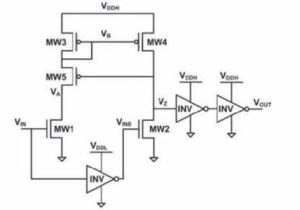
The NC7WZ17P6X chip is essentially a dual non-inverting buffer featuring Schmitt Trigger inputs, making it a solid choice for logic-level shifting. Even though the diagram you might see isn’t its exact internal circuit, it nicely illustrates how logic-level shifting typically works—something closely related to this chip’s practical uses.
Usually, you’d pick this chip when shifting signals from higher voltages (up to 5.5V) down to lower voltages (like from 5V to 3.3V). Its Schmitt Trigger inputs help keep your signals stable and clean, even in noisy environments.
The circuit example, however, demonstrates shifting from low voltage to high voltage using MOS transistors and inverters. While the NC7WZ17P6X primarily handles the opposite direction, the underlying principle—using transistor switching to reliably adjust voltage levels—is common to both setups. Understanding this general concept helps you effectively choose and apply logic-level shifting solutions in your designs.
nc7wz17p6x schmitt trigger application
The NC7WZ17P6X chip is great if you’re dealing with noisy or slow-changing signals because it has a built-in Schmitt Trigger. This means it clearly defines thresholds for rising and falling signals, making your output stable and jitter-free, even with messy inputs.
You’ll often find it useful in circuits like signal shaping, where it converts messy analog signals into clean digital square waves. It’s also excellent for button debouncing—those annoying little glitches when pressing mechanical switches. Just feed your button signal through this chip, and it’ll save your microcontroller from unnecessary software debouncing.
Additionally, with just a resistor and capacitor, you can easily create a stable oscillator for clock generation or timing applications.
Just remember: always keep input signals within clear voltage thresholds from the datasheet, avoid extremely slow signals hovering near thresholds, and place components close by to keep noise interference low.
nc7wz17p6x signal integrity example
If you’re dealing with messy or noisy signals in your circuits, the NC7WZ17P6X buffer chip can be a real lifesaver. Thanks to its built-in Schmitt Trigger inputs, it helps clean up signals by removing jitter and noise caused by slow changes or interference.
Imagine you have a clock line going to your microcontroller or FPGA that’s prone to interference due to long PCB traces or connectors. Pop this chip into your circuit, and you’ll instantly see clearer, more stable waveforms. It’s also great for cleaning up communication signals like SPI or I²C, making sure data stays accurate and stable.
Just make sure to keep the chip close to your signal source or receiver on your PCB layout to minimize path lengths. Also, avoid having your input signals hover around the chip’s switching thresholds for too long to maintain stable and reliable performance.
nc7wz17p6x buffer amplifier circuit
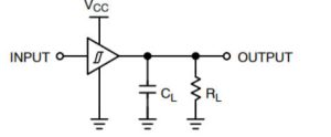
If you’re working on digital circuits and looking for a way to boost signal quality, the NC7WZ17P6X buffer amplifier is a solid choice. Think of this buffer as a helper—it isolates your input signal from the output load, so you won’t lose clarity even when driving heavier or capacitive loads.
The buffer’s high-impedance input ensures your original signal source isn’t disturbed. Internally, it uses built-in transistor stages to strengthen the signal, giving you a stable and reliable output. Typical applications include driving high-frequency or heavy loads and maintaining clean signals over longer PCB traces.
In practice, this means clearer, distortion-free outputs, which is crucial when handling sensitive digital signals. Just keep your load capacitors and resistors realistic, and you’ll have a buffer solution that noticeably improves your overall circuit performance.
Más como esto

LTC1955EUH
Dispositivos analógicos

PEX8718-AB80BI G
Broadcom / Avago

PCI6152-CC33BC
Broadcom / Avago

PCI9656-BA66BI G
Broadcom / Avago

PEX8619-BA50BC G
Broadcom / Avago

PCI6520-CB13BI G
Broadcom / Avago

PEX8747-CA80BC G
Broadcom / Avago

PEX8648-BB50BI F
Broadcom / Avago

PEX8609-BA50BC G
Broadcom / Avago
PEX8632-BB50RBC G
Broadcom / Avago

SII3132CNUTR
Enrejado

PEX8509-AA25BI G
Broadcom / Avago
Añadir también al carrito

TPS73HD325PWP
Texas Instruments

SN74LS14N
Texas Instruments

AL8860MP-13
Diodos incorporados

Ventilador 5331SX
Semiconductores Fairchild

JS28F640J3F75G
Tecnología Micron Inc.

STM32L4R5VIT6
STMicroelectrónica

LMV358DR2G
onsemi

FUSB302BUCX
onsemi

IR2101S
Tecnologías Infineon

PIC10F220T-I/OT
Tecnología de microchip

DSPIC33EP64MC506-I/PT
Tecnología de microchip

TLE8110EE
Tecnologías Infineon
Productos relacionados
LTC1955EUH
Dispositivos analógicos
PEX8718-AB80BI G
Broadcom / Avago
PCI6152-CC33BC
Broadcom / Avago
PCI9656-BA66BI G
Broadcom / Avago
PEX8619-BA50BC G
Broadcom / Avago
PCI6520-CB13BI G
Broadcom / Avago
PEX8747-CA80BC G
Broadcom / Avago
PEX8648-BB50BI F
Broadcom / Avago
PEX8609-BA50BC G
Broadcom / Avago
PEX8632-BB50RBC G
Broadcom / Avago
SII3132CNUTR
Enrejado
PEX8509-AA25BI G
Broadcom / Avago

PEX 8614-BA50BC
Broadcom / Avago
PEX8780-AB80BI G
Broadcom / Avago
PEX 8609-BA50BC
Broadcom / Avago

PCI9080-3G
Broadcom / Avago

PEX8618-BA50BC
Broadcom / Avago
PEX8648-BB50RBC G
Broadcom / Avago
PEX8680-AA50RBC G
Broadcom / Avago
PEX8608-BA50BC
Broadcom / Avago

PEX8749-CA80BC G
Broadcom / Avago
PEX8604-BA50BI G
Broadcom / Avago
PEX8716-CA80BC G
Broadcom / Avago
PEX8717-CA80BC G
Broadcom / Avago
PCI9054-AC50BI
Broadcom / Avago

OXPCIE954-FBAG
Broadcom / Avago
PCI 9054-AC50PI
Broadcom / Avago
PEX8619-BA50BI G
Broadcom / Avago
PEX8624-BB50RBC G
Broadcom / Avago
PEX8750-AB80BI G
Broadcom / Avago
Envíe RFQ, le responderemos de inmediato.
