PCBs Explained: How Printed Circuit Boards Power Electronics
Author:admin Date: 2025-03-21 09:16 Views:102
Introduction
Printed Circuit Boards (PCBs) are found in many electronics we use today. However, many people do not grasp the importance of PCBs and how they have revolutionized the manufacture and advancement of electronic devices.
With that in mind, what are printed circuit boards (PCBs)? Why are they even important?
A PCB (printed circuit board) is a board that forms a basis where electronic components are connected to each other by using copper traces/conductors. You can see how PCBs are vital for providing physical support to the electrical components and ensuring they remain connected at all times.
This guide aims to help you learn more about PCBs, their common terminology, the types available, their uses, and many other features. Ultimately, you should have a good grasp of what to expect with PCBs and possibly use them for your next project.
Parts of a PCB
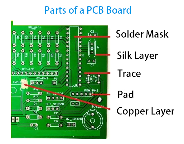
PCBs have four main parts. These parts are what determine the characteristics of the board. These parts include:
- Substrate: This material is made using fiberglass and is vital to provide the core strength that the PCB needs. It is basically the skeleton of the PCB, giving it the stability and strength it needs.
- Copper layer: The copper layer can consist of copper foil or coating depending on the choice of PCB type. Copper carries the electrical signals between the different components on the board.
- Solder mask: This polymer layer is vital for preventing the copper layer from oxidizing and the traces from breaking accidentally during PCB manufacturing.
- Silkscreen: This can be considered as the legend since it contains important information about the board and its components.
Roles of PCBs in Electronics
A PCB is an important foundation for modern electronics. For this reason, it is expected to have many roles. Here are some notable roles of PCBs.
– Mechanical support
Electronic devices need resistors, ICs, transistors, capacitors, and other components to work. They all need to be mounted somewhere. The PCB provides a stable platform for mechanical support for these components. Once mounted, they cannot move around, thus not affecting how the device works.
– Provide an electrical connection
The components on a PCB are interconnected via copper pathways or conductors. These pathways ensure a stable flow of electricity and signals. As such, they can be optimized during the design phase to ensure efficient performance of the components.
– Protection
PCBs are also vital for protecting the components mounted on them. This includes protection from excessive heat, interference, and environmental factors that can sometimes lead to failure.
– Versatile and scalable
Many forms and types of PCBs are on the market, including double-sided, single-sided, and multilayer. This allows you to choose the right board for your design requirements, which is why PCBs can be used to make simple and complex electronics simultaneously.
– Mass production and cost-effectiveness
PCBs are mainly used in the mass production of electronic devices because they are cost-effective. This means they can reduce manufacturing costs and ensure uniformity in performance and design. Since the boards are affordable, it is now easier for people to make all types of electronics.
Important PCB Terminology
Many terms will be heard during the design and manufacturing of a PCB. However, do you know what they mean? Below are common PCB terminologies to better understand the next time you hear them.
Layers – this is the number of conductive copper layers in a PCB. They range from 2 layers to over 20 layers.
Footprint – the number and arrangement of holes of an electronic component. This is what is used to make the electrical connection.
Track or Trace – this is the path that connects one component on the PCB to the other. It is used to carry electrical signals.
Solder Mask – this is the material covering the copper traces. Its function is to prevent the solder from flowing where it is not intended to go.
Silkscreen – these are the markings and text found on the PCB. Such content will provide key information, such as the component name or reference numbers.
Ground plane – this is the reference point for the electrical signals. It is hard to miss, thanks to its size.
Power plane – this is the copper area dedicated to carrying the electrical power to different components.
Schematic Symbol – this shows you the visual representation of how the different components on the PCB are connected.
These are just a few terms you may come across. However, you will learn more while working with the PCBs when handling various projects.
Key Components of PCBs and Functions

When you look at how to design a PCB, you will notice various key components that may not miss in any electronic device. As much as different electronic devices will have different uses, these components will be common. Here is what to expect as components of PCBs.
1. Resistors
Resistors limit the current flow in the circuit, acting as voltage dividers. Their working principle is vital for restricting the current flowing through sensitive components.
Resistor types include fixed resistors and potentiometers, which have variable resistance.
2. Capacitors
Capacitors are key for short-term energy storage. This is vital to maintaining steady power reaching the sensitive electronics in the circuit. Capacitors also smooth out voltage surges and filter noise, which is key in running the devices without issues.
3. Inductors
Inductors also store energy in the form of a magnetic field as electricity flows through them. They work with capacitors to filter the unwanted frequencies in the AC signals. Inductors are also vital for managing potential electromagnetic interference that could affect the circuit.
4. Transistors
The transistors on a PCB are vital for amplifying the signals and power in the circuit. They are common in modern electronics. Examples include bipolar junction transistors (BJTs) and field-effect transistors (FETs).
5. Diodes
Diodes are designed to only allow current flow in one direction. For this reason, they come in handy for rectification and signal processing in circuits. They can also be used to protect some sensitive electronics because of their characteristics.
6. Integrated Circuits
Integrated circuits (ICs) combine several components, such as transistors, resistors, and others, in one component. Because of this combination, you save on space and make the IC perform from basic to complex operations, depending on the design.
Types of PCBs
The type of PCB can determine how best to use it during the design process. We discuss some of the top PCBs on the market and where you can use them.
1. Single-Sided PCBs

This type of PCB has one side coded with the conducting material while the other is for mounting the electronic components.
This type of PCB was introduced in the 1950s but still has many applications today. This is because of its simple design, which still works for many uses.
A simple design also means fewer resources are used to make it. The result is having a low-cost PCB that still works quite well. You should still expect impressive performance even for being a single-sided PCB.
Applications
- Printers
- Vending machines
- Radio
- Stereo equipment, etc.
2. Double-Sided PCBs

For these PCBs, you get the conductive copper layer on both sides of the board. This means you can mount the components on either side of the board, and they will work. Because of this capability, such boards are mainly used to make more complex designs.
Having double layers for mounting components increases the use and flexibility of the board. You can now mount more components on the board than when using the single-sided board.
If you are working with a complex circuitry design, you need to get this. That is how you would see them used for lighting boards and car dashboards.
Applications
- Televisions
- Gaming consoles
- Digital cameras
- Audio devices
- Mobile phones
- Lighting systems
- HVAC Systems, etc.
3. Multi-layer PCBs
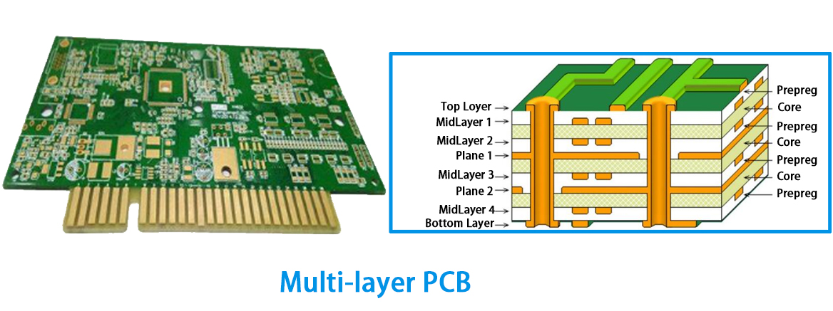
While most electronics are made with one or two conductive layers, you can get others with multiple layers. In this case, the PCB is manufactured to have several layers or base material. Expect such PCBs to have more than three conductive layers.
How are the multiple layers achieved? This is done using the sandwich model. This is where the conductive layers are separated using insulating material sheets. They are then bonded and laminated using high temperature and pressure, leaving no air gaps. You will now have a robust PCB after the assembly is done.
The multi-layer PCBs are expected to be more expensive than the other types mentioned above. However, depending on the application, they can still be essential or beneficial. For example, if you have to work with many components, you can expect to have a smaller footprint.
Applications
- 5G infrastructure
- Satellite communication
- Industrial controls
- Wearable devices
- Laptops, smartphones, tablets
- Diagnostic equipment, etc.
The PCBs mentioned above are the most common ways of categorizing them. However, you can come across other types of PCBs, such as rigid, flexible, HDI, etc. It all depends on the construction and application. Always consult with your supplier to understand the PCB you are buying and see if it aligns with what you are currently working on.
PCB Manufacturing Process

Before the PCB is installed in a device, various steps must be taken to actualize it. Below are the standard PCB manufacturing processes that you may go through.
1. PCB design
This part needs the use of PCB design software to help achieve the right design and one that works for you. Common PCB design software includes Eagle, KiCad, Altium Designer, and more.
Once the design is done, it is exported in a format the PCB board manufacturer supports.
2. The printing
Once the printing firm receives the design, it will proceed through the printing process. In this case, a plotter is used to print the photo films that will be attached to the PCB. Plotter printing is more common because it offers a more precise printing technology.
During this step, you end up with a plastic sheet containing the circuitry indicating where the copper traces will go on the PCB.
Excess copper is also removed during this step to reveal the copper paths. Layer alignment follows where the inner layers are aligned, and optical inspection is done to ensure accuracy and quality.
3. Lamination
The inner layers are now bonded using a pre-impregnated material. This is what forms the PCB core.
Next, holes are drilled into the PCB, outlining where the components will be attached or mounted.
4. Plating
More copper is deposited in the drilled holes to have electrical conductivity as part of plating.
The manufacturer then proceeds with outer layer imaging, in which the outer layer design is printed onto the copper-clad laminate.
Still, etching is done to remove the excess copper and create a cleaner outer layer design.
Silkscreening is also done during this stage. Here, the labels and markings are printed onto the PCB to identify and assemble the components easily.
5. Surface finishing
The PCB gets a final surface finish. This includes gold immersion and other types of protective coatings.
Once the surface finishing is complete, electrical testing follows to ensure the PCB works as expected.
A final inspection is done before the PCB components are assembled.
6. PCB assembly
During the PCB assembly process, the electronic components are attached to the PCB. The components are soldered and tested before they are shipped to the customer.
This is just a quick summary of how PCBs can be made. The actual process can be quite lengthy, with quality checks along the way. This is to ensure the quality and performance of the PCB are what you expect.
Design Considerations for PCBs
Many things go into designing PCBs correctly. If you find this being a possibility, consider the following:
- Consider short and direct signal paths if you want the best signal integrity. This helps minimize reflections and impedance.
- You should also work on thermal management. Place the heat-generating components in a way that allows for efficient heat dissipation.
- Also, consider the manufacturability of your design. This means the manufacturer should be able to make your design real. So, consider how easy it is to solder and probe as well.
- We still recommend designing a robust power distribution network. This allows for efficient, clean, and stable power delivery to all components.
- Shielding techniques can minimize electromagnetic interference and keep the device EMC-compliant.
- Consider design rules such as maintaining the correct trace widths, clearance, spacing, and other parameters. This should allow for better performance and manufacturability.
Conclusion
Electronics require PCBs to work correctly all the time. They provide a good backbone for setting up the various components that the devices need to function, including resistors, transistors, ICs, and many others. Depending on their application, you will encounter many types of PCBs. If you have to make your own PCB, make sure to work with reputable manufacturers to ensure they produce the right PCB that works according to the design.

