S8550 Transistor | PNP | Datasheet | Pinout MDD
- Transistor Type: PNP
- Current-Collector(Ic)(Max): 500 mA
- Voltage-Collector Emitter Breakdown (Max): 25 V
- Vce Saturation(Max)@IbIc: 600mV @ 50mA, 500mA
- Price: inquiry

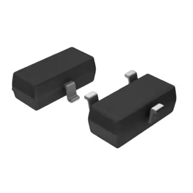
S8550 Pinout

S8550 Pinout Diagram
The S8550 is a PNP transistor commonly used in general-purpose switching and amplification applications. It has three main terminals: the Base, the Emitter, and the Collector. The transistor operates by controlling the current flow between these terminals, with the Base acting as the control input, the Emitter as the output, and the Collector as the input for current.
| Pin | Description | Function |
|---|---|---|
| 1 | Base | Controls current flow between the collector and emitter. The input pin. |
| 2 | Emitter | Current flows out of the transistor. Typically the output in a circuit. |
| 3 | Collector | Current enters the transistor. Acts as the input for current flow. |
The S8550 PNP transistor’s pinout consists of the Base (Pin 1), Emitter (Pin 2), and Collector (Pin 3). Understanding the function and description of these pins is essential for proper circuit design and operation, ensuring efficient performance in various electronic applications.
More Like This

MMBT2222A
HY Electronic (Cayman) Limited
MMBT3904
HY Electronic (Cayman) Limited
MMBT2907A
HY Electronic (Cayman) Limited

TIP41C
Rochester Electronics, LLC

PMBT3904,215
Rochester Electronics, LLC

TIP120
Central Semiconductor Corp

TIP36C
Central Semiconductor Corp
TIP35C
Central Semiconductor Corp

TIP3055
Central Semiconductor Corp
TIP2955
Central Semiconductor Corp
TIP147
Central Semiconductor Corp
TIP142
Central Semiconductor Corp
Also Add to Cart

MMBTA42-7-F
Diodes Incorporated
FJP13009H2TU
onsemi

2N3773
NTE Electronics, Inc

BDW93C
onsemi

MMBT2222A
Rochester Electronics, LLC

TIP32C
STMicroelectronics

BC847CLT1G
onsemi

BC846B
onsemi
TIP142
onsemi

FCX495TA
Diodes Incorporated

BCP56-10T1G
onsemi

2SC4617
onsemi,Rochester Electronics, LLC
MMBT2222A
HY Electronic (Cayman) Limited
MMBT3904
HY Electronic (Cayman) Limited
MMBT2907A
HY Electronic (Cayman) Limited
TIP41C
Rochester Electronics, LLC
PMBT3904,215
Rochester Electronics, LLC
TIP120
Central Semiconductor Corp
TIP36C
Central Semiconductor Corp
TIP35C
Central Semiconductor Corp
TIP3055
Central Semiconductor Corp
TIP2955
Central Semiconductor Corp